- Digital Electronics - Home
- Digital Electronics Basics
- Types of Digital Systems
- Types of Signals
- Logic Levels And Pulse Waveforms
- Digital System Components
- Digital Logic Operations
- Digital Systems Advantages
- Number Systems
- Number Systems
- Binary Numbers Representation
- Binary Arithmetic
- Signed Binary Arithmetic
- Octal Arithmetic
- Hexadecimal Arithmetic
- Complement Arithmetic
- Base Conversions
- Base Conversions
- Binary to Decimal Conversion
- Decimal to Binary Conversion
- Binary to Octal Conversion
- Octal to Binary Conversion
- Octal to Decimal Conversion
- Decimal to Octal Conversion
- Hexadecimal to Binary Conversion
- Binary to Hexadecimal Conversion
- Hexadecimal to Decimal Conversion
- Decimal to Hexadecimal Conversion
- Octal to Hexadecimal Conversion
- Hexadecimal to Octal Conversion
- Binary Codes
- Binary Codes
- 8421 BCD Code
- Excess-3 Code
- Gray Code
- ASCII Codes
- EBCDIC Code
- Code Conversion
- Error Detection & Correction Codes
- Logic Gates
- Logic Gates
- AND Gate
- OR Gate
- NOT Gate
- Universal Gates
- XOR Gate
- XNOR Gate
- CMOS Logic Gate
- OR Gate Using Diode Resistor Logic
- AND Gate vs OR Gate
- Two Level Logic Realization
- Threshold Logic
- Boolean Algebra
- Boolean Algebra
- Laws of Boolean Algebra
- Boolean Functions
- DeMorgan's Theorem
- SOP and POS Form
- POS to Standard POS Form
- Minimization Techniques
- K-Map Minimization
- Three Variable K-Map
- Four Variable K-Map
- Five Variable K-Map
- Six Variable K-Map
- Don't Care Condition
- Quine-McCluskey Method
- Min Terms and Max Terms
- Canonical and Standard Form
- Max Term Representation
- Simplification using Boolean Algebra
- Combinational Logic Circuits
- Digital Combinational Circuits
- Digital Arithmetic Circuits
- Multiplexers
- Multiplexer Design Procedure
- Mux Universal Gate
- 2-Variable Function Using 4:1 Mux
- 3-Variable Function Using 8:1 Mux
- Demultiplexers
- Mux vs Demux
- Parity Bit Generator and Checker
- Comparators
- Encoders
- Keyboard Encoders
- Priority Encoders
- Decoders
- Arithmetic Logic Unit
- 7-Segment LED Display
- Code Converters
- Code Converters
- Binary to Decimal Converter
- Decimal to BCD Converter
- BCD to Decimal Converter
- Binary to Gray Code Converter
- Gray Code to Binary Converter
- BCD to Excess-3 Converter
- Excess-3 to BCD Converter
- Adders
- Half Adders
- Full Adders
- Serial Adders
- Parallel Adders
- Full Adder using Half Adder
- Half Adder vs Full Adder
- Full Adder with NAND Gates
- Half Adder with NAND Gates
- Binary Adder-Subtractor
- Subtractors
- Half Subtractors
- Full Subtractors
- Parallel Subtractors
- Full Subtractor using 2 Half Subtractors
- Half Subtractor using NAND Gates
- Sequential Logic Circuits
- Digital Sequential Circuits
- Clock Signal and Triggering
- Latches
- Shift Registers
- Shift Register Applications
- Binary Registers
- Bidirectional Shift Register
- Counters
- Binary Counters
- Non-binary Counter
- Design of Synchronous Counter
- Synchronous vs Asynchronous Counter
- Finite State Machines
- Algorithmic State Machines
- Flip Flops
- Flip-Flops
- Conversion of Flip-Flops
- D Flip-Flops
- JK Flip-Flops
- T Flip-Flops
- SR Flip-Flops
- Clocked SR Flip-Flop
- Unclocked SR Flip-Flop
- Clocked JK Flip-Flop
- JK to T Flip-Flop
- SR to JK Flip-Flop
- Triggering Methods:Flip-Flop
- Edge-Triggered Flip-Flop
- Master-Slave JK Flip-Flop
- Race-around Condition
- A/D and D/A Converters
- Analog-to-Digital Converter
- Digital-to-Analog Converter
- DAC and ADC ICs
- Realization of Logic Gates
- NOT Gate from NAND Gate
- OR Gate from NAND Gate
- AND Gate from NAND Gate
- NOR Gate from NAND Gate
- XOR Gate from NAND Gate
- XNOR Gate from NAND Gate
- NOT Gate from NOR Gate
- OR Gate from NOR Gate
- AND Gate from NOR Gate
- NAND Gate from NOR Gate
- XOR Gate from NOR Gate
- XNOR Gate from NOR Gate
- NAND/NOR Gate using CMOS
- Full Subtractor using NAND Gate
- AND Gate Using 2:1 MUX
- OR Gate Using 2:1 MUX
- NOT Gate Using 2:1 MUX
- Memory Devices
- Memory Devices
- RAM and ROM
- Cache Memory Design
- Programmable Logic Devices
- Programmable Logic Devices
- Programmable Logic Array
- Programmable Array Logic
- Field Programmable Gate Arrays
- Digital Electronics Families
- Digital Electronics Families
- CPU Architecture
- CPU Architecture
Universal Gates NAND and NOR
A logic gate that can implement any kind of possible Boolean function is called a universal gate. There are two universal logic gates namely, NAND gate and NOR gate.
These two gates are called universal gates because they can perform the function of any other logic gate like AND, OR, NOT, XOR, and XNOR without need of any other type of logic gate. For example, we can perform the AND gate function by using only NAND gates or only NOR gates.
In this chapter, we will study the theory and working of the universal gates, i.e., NAND gate and NOR gate.
What is a NAND Gate?
The NAND gate is a universal gate that basically a combination of two basic logic gates namely, AND gate and NOT gate. It is designed by connecting a NOT gate to the output line of the AND gate, as shown in the following figure.

The NAND gate can have two or more input lines and one output line. The output of the NAND gate is low or logic 0 only when all its inputs are high or logic 1. Otherwise, the output of the NAND gate is high or logic 1.
The NAND gate is basically a logic gate that performs the inverse operation of an AND gate.
Being a universal gate, the NAND gate can implement any possible Boolean function or operation of any other type of logic gate.
Logic Symbol of NAND Gate
The logic symbols of a two-input and three-input NAND gates are depicted in the following figure.

Here, the bubble at the output side represents the inversion operation.
The variables A, B, and C designate the input lines and the variable Y represents the output line of the NAND gate.
Truth Table of NAND Gate
Truth table is a table of inputs and outputs of a NAND gate showing the relationship between them. Here is the truth table of a two-input NAND gate −
| Input | Output | |
|---|---|---|
| A | B | Y |
| 0 | 0 | 1 |
| 0 | 1 | 1 |
| 1 | 0 | 1 |
| 1 | 1 | 0 |
The truth table for a three-input NAND gate is given below −
| Input | Output | ||
|---|---|---|---|
| A | B | C | Y |
| 0 | 0 | 0 | 1 |
| 0 | 0 | 1 | 1 |
| 0 | 1 | 0 | 1 |
| 0 | 1 | 1 | 1 |
| 1 | 0 | 0 | 1 |
| 1 | 0 | 1 | 1 |
| 1 | 1 | 0 | 1 |
| 1 | 1 | 1 | 0 |
From these two truth tables, we can observe that the NAND gate produces a low or logic 0 output only when all its inputs are high or logic 1. For any other input combinations, the output is high or logic 1.
Boolean Expression of NAND Gate
The Boolean expression is a logical function that describes the logical relationship between inputs and output of a NAND gate.
The Boolean expression for a two-input NAND gate is give below −
$$\mathrm{Y \: = \: \overline{AB} \: = \: (AB)'}$$
The Boolean expression for a three-input NAND gate is given by,
$$\mathrm{Y \: = \: \overline{ABC} \: = \: (ABC)'}$$
Here, A, B, and C are the input variables and Y is the output variable.
Working of NAND Gate
The working of a two-input NAND gate for different input combinations is described below −
- If A = 0 and B = 0, the output of the NAND gate is Y = 1.
- If A = 0 and B = 1, the output of the NAND gate is Y = 1.
- If A = 1 and B = 0, the output of the NAND gate is Y = 1.
- If A = 1 and B = 1, the output of the NAND gate is Y = 0.
Similarly, the working of a three-input NAND gate can be explained as below −
- If A = 0, B = 0, and C = 0 the output of the NAND gate is Y = 1.
- If A = 0, B = 0, and C = 1 the output of the NAND gate is Y = 1.
- If A = 0, B = 1, and C = 0 the output of the NAND gate is Y = 1.
- If A = 0, B = 1, and C = 1 the output of the NAND gate is Y = 1.
- If A = 1, B = 0, and C = 0 the output of the NAND gate is Y = 1.
- If A = 1, B = 0, and C = 1 the output of the NAND gate is Y = 1.
- If A = 1, B = 1, and C = 0 the output of the NAND gate is Y = 1.
- If A = 1, B = 1, and C = 1 the output of the NAND gate is Y = 0.
This is all about the operation of a NAND gate for different input combinations.
It is also important to note that in this chapter, we are discussing the theory of NAND gate by considering only two and three input variables. But the same logic and theory is applicable to any number of inputs.
NAND Gate using Transistor
We can implement the NAND gate logic by using BJT transistors. Such a NAND gate is referred to as a transistor NAND gate.
The transistor circuit diagram of a two-input NAND gate is shown in the following figure.
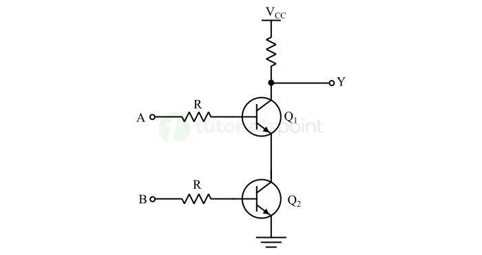
Working of Transistor NAND Gate
The working of this transistor NAND gate for different input combinations is explained below −
When both inputs A and B are connected to a low signal, the transistors Q1 and Q2 act as open switches. The entire supply voltage will appear at the output line Y. Hence, for this input combination, the output of the circuit is high or logic 1.
When the input A is at low level and the input B is at high level, the transistor Q1 acts as an open switch and the transistor Q2 acts as a closed switch. In this case, there is not a direct connection between power supply and the ground terminal. Hence, the whole supply voltage will appear at the output terminal Y, making it high or logic 1.
When the input A is at high level and the input B is at low level, the transistor Q1 acts as a closed switch and the transistor Q2 acts as an open switch. Again, there is a disconnection between power supply and the ground terminal. For this combination of inputs, the entire supply voltage will appear at the output line and sets the output high or logic 1.
When the both inputs are connected to a high or logic 1 signal, both transistors will turn on and connects the output line directly to the ground terminal i.e., to a low potential. This makes the output of the circuit low or logic 0.
Hence, the output of this circuit is low or logic 0, only when all inputs are high or logic 1, otherwise the output is high or logic 1. Thus, this circuit implements the NAND gate logic.
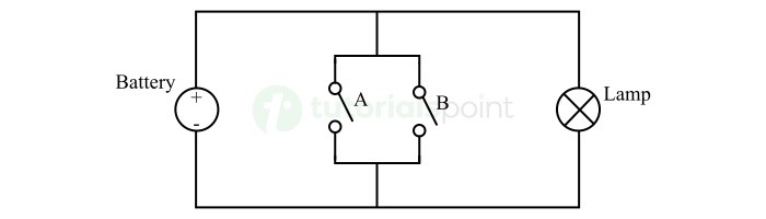
NAND Gate using Switches
We can also realize the NAND gate using electric switches, a battery, and a lamp. The circuit diagram of a two-input NAND gate using switches is shown in the following figure.
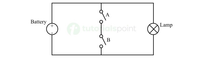
In this switching circuit, when both switches A and B are closed, there is a short-circuited path for the flow of electric current that bypasses the lamp. Hence, no current will flow through the lamp and the lamp will not glow. This represents the low or logic 0 output.
For any other switching arrangement, such as A is closed and B is open, A is open and B is closed, or A and B are open. There is no short-circuited path and the entire current will flow through the lamp, making it turn on. This represents the high or logic 1 output.
Thus, the output of this switching circuit is low or logic 0 only when both switches are closed, otherwise the output is high or logic 1. Hence, this circuit acts as a NAND gate.
We can add more switches in series with A and B to implement a higher order NAND gate.
NAND Gate as an Inverter
The NAND gate can also be used as an inverter gate. For this, all its inputs are joined together and the input signal to be inverted is applied to the common terminal as shown in the following figure.

Applications of NAND Gate
The NAND gate is used in a variety of digital and automated systems. Some of them are listed below −
- Alarm circuits
- Buzzer and burglar devices
- Automatic temperature regulation systems
- Security systems
- Automated doors and windows, etc.
This is all about the NAND gate, its working and applications. Let us now discuss the theory of another universal gate named, NOR gate.
What is a NOR Gate?
The NOR gate is another universal gate used in digital electronics to implement Boolean functions. It is a combination of two basic logic gates namely, OR gate and NOT gate. The NOR gate is designed by connecting a NOT gate to the output line and the final output is taken from the output line of the NOT gate as shown in the following figure.

Being a universal logic gate, it can be used to implement any possible Boolean function or the other logic gates single-handedly.
The NOR gate can have two or more input lines and one output line. The output of the NOR gate is high or logic 1 only when all its inputs are low or logic 0. For all other input combinations, the output of the NOR gate is low or logic 0.
Logic Symbol of NOR Gate
The logic symbols of a two-input and three-input NOR gates are shown in the following figure.
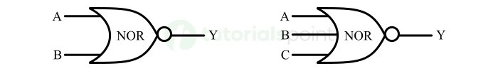
Here, A, B, and C are the input lines and Y is the output line. The bubble at the output end represents the inversion operation.
Truth Table of NOR Gate
The truth table of the NOR gate specifies the output for different input combinations. The truth table of a two-input NOR gate is given below −
| Input | Output | |
|---|---|---|
| A | B | Y |
| 0 | 0 | 1 |
| 0 | 1 | 0 |
| 1 | 0 | 0 |
| 1 | 1 | 0 |
The following is the truth table of a three-input NOR gate −
| Input | Output | ||
|---|---|---|---|
| A | B | C | Y |
| 0 | 0 | 0 | 1 |
| 0 | 0 | 1 | 0 |
| 0 | 1 | 0 | 0 |
| 0 | 1 | 1 | 0 |
| 1 | 0 | 0 | 0 |
| 1 | 0 | 1 | 0 |
| 1 | 1 | 0 | 0 |
| 1 | 1 | 1 | 0 |
From these truth tables, we can observe that the output of the NOR gate is high or logic 1 only when all its inputs are low or logic 0, otherwise the output is low or logic 0.
Working of NOR Gate
The operation of a two-input NOR gate for all possible input combinations is explained below −
- If A = 0 and B = 0, the output of the NOR gate is Y = 1.
- If A = 0 and B = 1, the output of the NOR gate is Y = 0.
- If A = 1 and B = 0, the output of the NOR gate is Y = 0.
- If A = 1 and B = 1, the output of the NOR gate is Y = 0.
Similarly, the operation of the three-input NOR gate can be described, as below −
- If A = 0, B = 0, and C = 0 the output of the NOR gate is Y = 1.
- If A = 0, B = 0, and C = 1 the output of the NOR gate is Y = 0.
- If A = 0, B = 1, and C = 0 the output of the NOR gate is Y = 0.
- If A = 0, B = 1, and C = 1 the output of the NOR gate is Y = 0.
- If A = 1, B = 0, and C = 0 the output of the NOR gate is Y = 0.
- If A = 1, B = 0, and C = 1 the output of the NOR gate is Y = 0.
- If A = 1, B = 1, and C = 0 the output of the NOR gate is Y = 0.
- If A = 1, B = 1, and C = 1 the output of the NOR gate is Y = 0.
From this discussion, we can observe that the NOR gate produces a high or logic 1 output when all its inputs are low or logic 0.
NOR Gate using Transistor
We can implement the NOR gate using transistors. The circuit diagram of a two-input NOR gate using transistors is shown in the following figure. This circuit is known as transistor NOR gate.
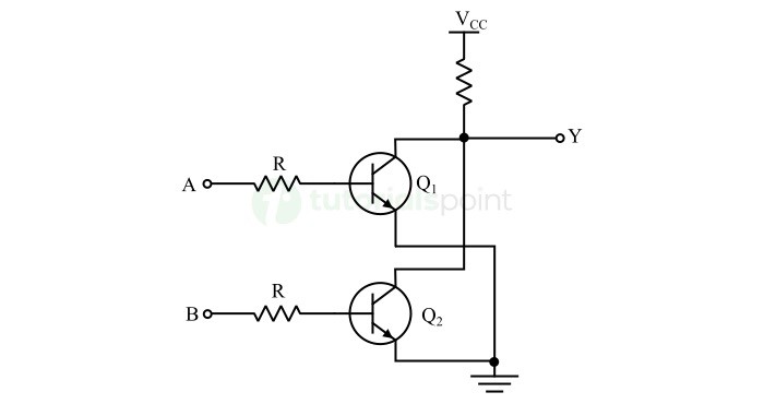
Working of Transistor NOR Gate
The working of the transistor NOR gate is explained below −
When both inputs A and B are low, the transistors Q1 and Q2 do not conduct and act as open switches. In this case, the output line Y will directly connect to the power supply. Thus, the whole supply voltage will appear at the output terminal. This makes the output of the circuit high or logic 1.
When the input A is connected to low and the input B is connected to a high signal, the transistor Q1 will act as an open switch while the transistor Q2 will act as a closed switch. In this case, the output line Y will directly connect to the ground terminal through the transistor Q2. This results in a low signal at the output line.
When the input A is connected to high and the input B is connected to a low signal, the transistor Q1 will conduct and the transistor Q2 will act as an open switch. In this case, the output line is directly connected to the ground terminal. Thus, the output is low or logic 0.
When both inputs A and B are connected to a high signal, both transistors Q1 and Q2 will act as closed switches and connect the output line directly to the ground terminal. In the case also, the output is low or logic 0.
From this discussion, we can observe that this transistor circuit implements the NOR logic and hence called as transistor NOR gate.
We can add more transistors to the circuit to obtain a higher order NOR gate.
NOR Gate using Switches
We can also realize the NOR gate using electrical switches. A circuit diagram for a two-input NOR gate using switches is shown in the following figure.
In this circuit, if both switches A and B are open, the entire current flows through the lamp and turn it on. This represents the high or logic 1 state of the output.
If both or any of the switches is closed, there is a short-circuited path for the flow of current that bypasses the lamp. In this case, the lamp will not glow and represent the low or logic 0 state of the output.
Thus, the output of this switching circuit is high or logic 1, only when both of its inputs are low i.e., open switches, otherwise the output is low or logic 0.
Therefore, this electric circuit realizes the NOR gate operation and logic.
NOR Gate as an Inverter
The NOR gate also be operated as an inverter gate. To use the NOR gate as an inverter, all its inputs are connected together and the input signal is applied to the common terminal as shown in the following figure.

Applications of NOR Gate
The NOR gate is used in numerous digital systems. Some common applications of NOR gate are listed below −
- Various digital systems
- Industrial automation and control systems
- Traffic control systems
- Alarm circuits
- Digital arithmetic circuits like adders and subtractors, etc.
Conclusion
In conclusion, a universal logic gate is one that can implement any possible Boolean functions or other logic gates without need of any other type of logic gates. In digital electronics, there are two universal logic gates namely, NAND gate and NOR gate.
In this chapter, we explained the theory, working, and applications of these two universal gates. Here, we covered only two and three-input NAND and NOR gates, but the same theory and explanation is equally valid for NAND and NOR gates with more than three inputs.