- Digital Electronics - Home
- Digital Electronics Basics
- Types of Digital Systems
- Types of Signals
- Logic Levels And Pulse Waveforms
- Digital System Components
- Digital Logic Operations
- Digital Systems Advantages
- Number Systems
- Number Systems
- Binary Numbers Representation
- Binary Arithmetic
- Signed Binary Arithmetic
- Octal Arithmetic
- Hexadecimal Arithmetic
- Complement Arithmetic
- Base Conversions
- Base Conversions
- Binary to Decimal Conversion
- Decimal to Binary Conversion
- Binary to Octal Conversion
- Octal to Binary Conversion
- Octal to Decimal Conversion
- Decimal to Octal Conversion
- Hexadecimal to Binary Conversion
- Binary to Hexadecimal Conversion
- Hexadecimal to Decimal Conversion
- Decimal to Hexadecimal Conversion
- Octal to Hexadecimal Conversion
- Hexadecimal to Octal Conversion
- Binary Codes
- Binary Codes
- 8421 BCD Code
- Excess-3 Code
- Gray Code
- ASCII Codes
- EBCDIC Code
- Code Conversion
- Error Detection & Correction Codes
- Logic Gates
- Logic Gates
- AND Gate
- OR Gate
- NOT Gate
- Universal Gates
- XOR Gate
- XNOR Gate
- CMOS Logic Gate
- OR Gate Using Diode Resistor Logic
- AND Gate vs OR Gate
- Two Level Logic Realization
- Threshold Logic
- Boolean Algebra
- Boolean Algebra
- Laws of Boolean Algebra
- Boolean Functions
- DeMorgan's Theorem
- SOP and POS Form
- POS to Standard POS Form
- Minimization Techniques
- K-Map Minimization
- Three Variable K-Map
- Four Variable K-Map
- Five Variable K-Map
- Six Variable K-Map
- Don't Care Condition
- Quine-McCluskey Method
- Min Terms and Max Terms
- Canonical and Standard Form
- Max Term Representation
- Simplification using Boolean Algebra
- Combinational Logic Circuits
- Digital Combinational Circuits
- Digital Arithmetic Circuits
- Multiplexers
- Multiplexer Design Procedure
- Mux Universal Gate
- 2-Variable Function Using 4:1 Mux
- 3-Variable Function Using 8:1 Mux
- Demultiplexers
- Mux vs Demux
- Parity Bit Generator and Checker
- Comparators
- Encoders
- Keyboard Encoders
- Priority Encoders
- Decoders
- Arithmetic Logic Unit
- 7-Segment LED Display
- Code Converters
- Code Converters
- Binary to Decimal Converter
- Decimal to BCD Converter
- BCD to Decimal Converter
- Binary to Gray Code Converter
- Gray Code to Binary Converter
- BCD to Excess-3 Converter
- Excess-3 to BCD Converter
- Adders
- Half Adders
- Full Adders
- Serial Adders
- Parallel Adders
- Full Adder using Half Adder
- Half Adder vs Full Adder
- Full Adder with NAND Gates
- Half Adder with NAND Gates
- Binary Adder-Subtractor
- Subtractors
- Half Subtractors
- Full Subtractors
- Parallel Subtractors
- Full Subtractor using 2 Half Subtractors
- Half Subtractor using NAND Gates
- Sequential Logic Circuits
- Digital Sequential Circuits
- Clock Signal and Triggering
- Latches
- Shift Registers
- Shift Register Applications
- Binary Registers
- Bidirectional Shift Register
- Counters
- Binary Counters
- Non-binary Counter
- Design of Synchronous Counter
- Synchronous vs Asynchronous Counter
- Finite State Machines
- Algorithmic State Machines
- Flip Flops
- Flip-Flops
- Conversion of Flip-Flops
- D Flip-Flops
- JK Flip-Flops
- T Flip-Flops
- SR Flip-Flops
- Clocked SR Flip-Flop
- Unclocked SR Flip-Flop
- Clocked JK Flip-Flop
- JK to T Flip-Flop
- SR to JK Flip-Flop
- Triggering Methods:Flip-Flop
- Edge-Triggered Flip-Flop
- Master-Slave JK Flip-Flop
- Race-around Condition
- A/D and D/A Converters
- Analog-to-Digital Converter
- Digital-to-Analog Converter
- DAC and ADC ICs
- Realization of Logic Gates
- NOT Gate from NAND Gate
- OR Gate from NAND Gate
- AND Gate from NAND Gate
- NOR Gate from NAND Gate
- XOR Gate from NAND Gate
- XNOR Gate from NAND Gate
- NOT Gate from NOR Gate
- OR Gate from NOR Gate
- AND Gate from NOR Gate
- NAND Gate from NOR Gate
- XOR Gate from NOR Gate
- XNOR Gate from NOR Gate
- NAND/NOR Gate using CMOS
- Full Subtractor using NAND Gate
- AND Gate Using 2:1 MUX
- OR Gate Using 2:1 MUX
- NOT Gate Using 2:1 MUX
- Memory Devices
- Memory Devices
- RAM and ROM
- Cache Memory Design
- Programmable Logic Devices
- Programmable Logic Devices
- Programmable Logic Array
- Programmable Array Logic
- Field Programmable Gate Arrays
- Digital Electronics Families
- Digital Electronics Families
- CPU Architecture
- CPU Architecture
Digital Electronics - Serial Binary Adder
In digital electronics, the binary adder is a combinational logic circuit which performs the addition of two or more binary digits. The binary addition is performed based on the Boolean algebraic laws of addition, i.e.,
$$\mathrm{0 \: + \: 0 \: = \: 0}$$
$$\mathrm{0 \: + \: 1 \: = \: 1}$$
$$\mathrm{1 \: + \: 0 \: = \: 1}$$
$$\mathrm{1 \: + \: 1 \: = \: 0}$$
Binary adders are classified into two types namely, serial binary adder and parallel binary adder.
In this tutorial, we will discuss serial binary adder, its definition, logic circuit diagram, and operation. So, let us start with basic introduction of serial binary adder.
What is a Serial Binary Adder?
A serial binary adder is a binary adder circuit which is used to add binary numbers in serial form. In the serial adder, the two binary numbers which are added serially are stored in two shift registers, let shift register A and shift register B.
The logic circuit diagram of the serial binary adder is shown in Figure 1.
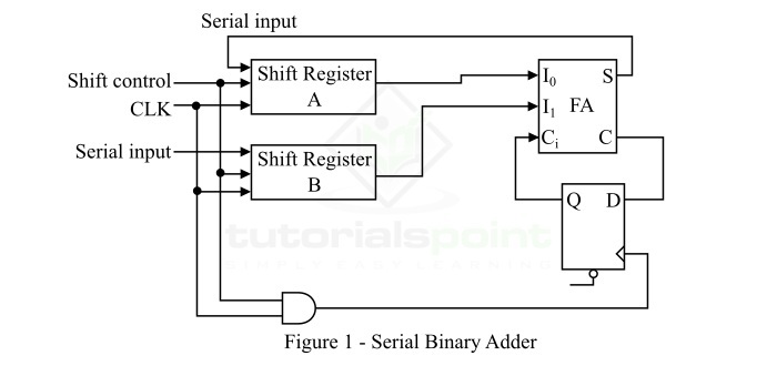
The function of different elements of the serial adder circuit is as follows −
Full Adder
Full adder is a digital combinational logic circuit which can add three binary digits and can produce two output bits, i.e. sum bit and carry bit. In the serial binary adder circuit, the full adder adds one pair of bits at a time.
Shift Register
A group of flip-flops that can store several bits of data is called a shift register. In serial binary adder, two shift registers are used, where one is for storing augend bit and the other is for storing added of the binary number.
D Flip-Flop
In serial adder, the D flip-flop is used to store the carry output bit. The output of this D flip-flop is used as the carry input in the next stage of addition.
Operation of Series Binary Adder
In the serial binary adder circuit, the binary digits (bits) are added one pair at a time using a full-adder circuit. The carry generated from the full adder is transferred to a D-flip flop. Thus, the output of this D-flip flop is then used as the carry input for the next pair of significant bits. The sum bit S is transferred to a third shift register. Now, let us understand the operation of the serial binary adder in the detail.
At beginning, the shift register A stores the augend bit of the given binary number, and the shift register B stores the addend bit. Initially, the D flip flop is cleared to 0, hence no carry bit is present. The outputs of shift registers A and B supply a pair of significant bits to the full adder circuit at inputs I0 and I1. A shift control is used to enable the shift registers A and B and the carry flip-flop.
Therefore, at each clock pulse, the registers A and B are shifted to the right, and the sum bit from output S of the full adder circuit enters the left most of the shift register A. Thus, for each succeeding clock pulse a new sum bit is transferred to the shift register A and a new carry bit is transferred to the output Q of the D flip flop. This process continues until the shift control is disabled.
Hence, the addition of two binary numbers in serial form is accomplished by supplying a pair of bits together with the previous carry to a full adder circuit, and transferring a sum bit at a time into the shift register A.
Now, we can summarize the working process of the serial binary adder as follows −
- Initially, the shift register A and the carry flip flop are set to 0, and the first number is added from the register B.
- When the register B is shifting through the full adder, a second number is transferred to it through its serial input.
- This second number is then added to the number of the register A, while a third number is transferred to into the register B through the serial input.
This process is executed repeatedly to perform the addition of two, three, or more binary number in serial form and accumulate the sum result in the shift register A.