- Digital Electronics - Home
- Digital Electronics Basics
- Types of Digital Systems
- Types of Signals
- Logic Levels And Pulse Waveforms
- Digital System Components
- Digital Logic Operations
- Digital Systems Advantages
- Number Systems
- Number Systems
- Binary Numbers Representation
- Binary Arithmetic
- Signed Binary Arithmetic
- Octal Arithmetic
- Hexadecimal Arithmetic
- Complement Arithmetic
- Base Conversions
- Base Conversions
- Binary to Decimal Conversion
- Decimal to Binary Conversion
- Binary to Octal Conversion
- Octal to Binary Conversion
- Octal to Decimal Conversion
- Decimal to Octal Conversion
- Hexadecimal to Binary Conversion
- Binary to Hexadecimal Conversion
- Hexadecimal to Decimal Conversion
- Decimal to Hexadecimal Conversion
- Octal to Hexadecimal Conversion
- Hexadecimal to Octal Conversion
- Binary Codes
- Binary Codes
- 8421 BCD Code
- Excess-3 Code
- Gray Code
- ASCII Codes
- EBCDIC Code
- Code Conversion
- Error Detection & Correction Codes
- Logic Gates
- Logic Gates
- AND Gate
- OR Gate
- NOT Gate
- Universal Gates
- XOR Gate
- XNOR Gate
- CMOS Logic Gate
- OR Gate Using Diode Resistor Logic
- AND Gate vs OR Gate
- Two Level Logic Realization
- Threshold Logic
- Boolean Algebra
- Boolean Algebra
- Laws of Boolean Algebra
- Boolean Functions
- DeMorgan's Theorem
- SOP and POS Form
- POS to Standard POS Form
- Minimization Techniques
- K-Map Minimization
- Three Variable K-Map
- Four Variable K-Map
- Five Variable K-Map
- Six Variable K-Map
- Don't Care Condition
- Quine-McCluskey Method
- Min Terms and Max Terms
- Canonical and Standard Form
- Max Term Representation
- Simplification using Boolean Algebra
- Combinational Logic Circuits
- Digital Combinational Circuits
- Digital Arithmetic Circuits
- Multiplexers
- Multiplexer Design Procedure
- Mux Universal Gate
- 2-Variable Function Using 4:1 Mux
- 3-Variable Function Using 8:1 Mux
- Demultiplexers
- Mux vs Demux
- Parity Bit Generator and Checker
- Comparators
- Encoders
- Keyboard Encoders
- Priority Encoders
- Decoders
- Arithmetic Logic Unit
- 7-Segment LED Display
- Code Converters
- Code Converters
- Binary to Decimal Converter
- Decimal to BCD Converter
- BCD to Decimal Converter
- Binary to Gray Code Converter
- Gray Code to Binary Converter
- BCD to Excess-3 Converter
- Excess-3 to BCD Converter
- Adders
- Half Adders
- Full Adders
- Serial Adders
- Parallel Adders
- Full Adder using Half Adder
- Half Adder vs Full Adder
- Full Adder with NAND Gates
- Half Adder with NAND Gates
- Binary Adder-Subtractor
- Subtractors
- Half Subtractors
- Full Subtractors
- Parallel Subtractors
- Full Subtractor using 2 Half Subtractors
- Half Subtractor using NAND Gates
- Sequential Logic Circuits
- Digital Sequential Circuits
- Clock Signal and Triggering
- Latches
- Shift Registers
- Shift Register Applications
- Binary Registers
- Bidirectional Shift Register
- Counters
- Binary Counters
- Non-binary Counter
- Design of Synchronous Counter
- Synchronous vs Asynchronous Counter
- Finite State Machines
- Algorithmic State Machines
- Flip Flops
- Flip-Flops
- Conversion of Flip-Flops
- D Flip-Flops
- JK Flip-Flops
- T Flip-Flops
- SR Flip-Flops
- Clocked SR Flip-Flop
- Unclocked SR Flip-Flop
- Clocked JK Flip-Flop
- JK to T Flip-Flop
- SR to JK Flip-Flop
- Triggering Methods:Flip-Flop
- Edge-Triggered Flip-Flop
- Master-Slave JK Flip-Flop
- Race-around Condition
- A/D and D/A Converters
- Analog-to-Digital Converter
- Digital-to-Analog Converter
- DAC and ADC ICs
- Realization of Logic Gates
- NOT Gate from NAND Gate
- OR Gate from NAND Gate
- AND Gate from NAND Gate
- NOR Gate from NAND Gate
- XOR Gate from NAND Gate
- XNOR Gate from NAND Gate
- NOT Gate from NOR Gate
- OR Gate from NOR Gate
- AND Gate from NOR Gate
- NAND Gate from NOR Gate
- XOR Gate from NOR Gate
- XNOR Gate from NOR Gate
- NAND/NOR Gate using CMOS
- Full Subtractor using NAND Gate
- AND Gate Using 2:1 MUX
- OR Gate Using 2:1 MUX
- NOT Gate Using 2:1 MUX
- Memory Devices
- Memory Devices
- RAM and ROM
- Cache Memory Design
- Programmable Logic Devices
- Programmable Logic Devices
- Programmable Logic Array
- Programmable Array Logic
- Field Programmable Gate Arrays
- Digital Electronics Families
- Digital Electronics Families
- CPU Architecture
- CPU Architecture
Full Adder in Digital Electronics
What is a Full Adder?
A combinational logic circuit that can add two binary digits (bits) and a carry bit, and produces a sum bit and a carry bit as output is known as a full-adder.
In other words, a combinational circuit which is designed to add three binary digits and produces two outputs (sum and carry) is known as a full adder. Thus, a full adder circuit adds three binary digits, where two are the inputs and one is the carry forwarded from the previous addition. The block diagram and circuit diagram of the full adder are shown in Figure-1.
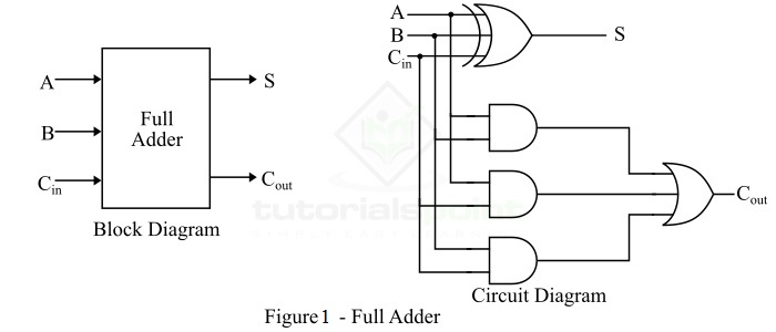
Hence, the circuit of the full adder consists of one EX-OR gate, three AND gates and one OR gate, which are connected together as shown in the full adder circuit in Figure-1.
Operation of Full Adder
Full adder takes three inputs namely A, B, and Cin. Where, A and B are the two binary digits, and Cin is the carry bit from the previous stage of binary addition. The sum output of the full adder is obtained by XORing the bits A, B, and Cin. While the carry output bit (Cout) is obtained using AND and OR operations.
Truth Table of Full Adder
Truth table is one that indicates the relationship between input and output variables of a logic circuit and explains the operation of the logic circuit. The following is the truth table of the full-adder circuit −
| Inputs | Outputs | |||
|---|---|---|---|---|
| A | B | Cin | S (Sum) | Cout (Carry) |
| 0 | 0 | 0 | 0 | 0 |
| 0 | 0 | 1 | 1 | 0 |
| 0 | 1 | 0 | 1 | 0 |
| 0 | 1 | 1 | 0 | 1 |
| 1 | 0 | 0 | 1 | 0 |
| 1 | 0 | 1 | 0 | 1 |
| 1 | 1 | 0 | 0 | 1 |
| 1 | 1 | 1 | 1 | 1 |
Hence, from the truth table, it is clear that the sum output of the full adder is equal to 1 when only 1 input is equal to 1 or when all the inputs are equal to 1. While the carry output has a carry of 1 if two or three inputs are equal to 1.
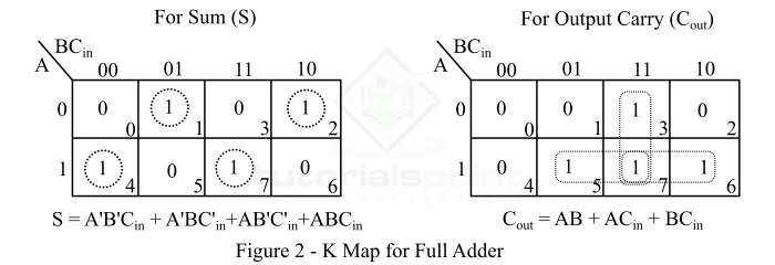
K-Map for Full Adder
K-Map (Karnaugh Map) is a tool for simplifying binary complex Boolean algebraic expressions. The K-Map for full adder is shown in Figure-2.
Characteristic Equations of Full Adder
The characteristic equations of the full adder, i.e. equations of sum (S) and carry output (Cout) are obtained according to the rules of binary addition. These equations are given below −
The sum (S) of the full-adder is the XOR of A, B, and Cin. Therefore,
$$\mathrm{Sum, \: S \: = \: A \: \oplus \: B \: \oplus \: C_{in} \: = \: A'B'C_{in} \: + \: A'BC'_{in} \: + \: AB'C'_{in} \: + \: ABC_{in} }$$
The carry (C) of the half-adder is the AND of A and B. Therefore,
$$\mathrm{Carry, \: C \: = \: AB \: + \: AC_{in} \: + \: BC_{in}}$$
Advantages of Full Adder
The following are the important advantages of full adder over half adder −
- Full adder provides facility to add the carry from the previous stage.
- The power consumed by the full adder is relatively less as compared to half adder.
- Full adder can be easily converted into a half subtractor just by adding a NOT gate in the circuit.
- Full adder produces higher output that half adder.
- Full adder is one of the essential part of critic digital circuits like multiplexers.
- Full adder performs operation at higher speed.
Applications of Full Adder
The following are the important applications of full adder −
- Full adders are used in ALUs (arithmetic logic units) of CPUs of computers.
- Full adders are used in calculators.
- Full adders also help in carrying out multiplication of binary numbers.
- Full adders are also used to realize critic digital circuits like multiplexers.
- Full adders are used to generate memory addresses.
- Full adders are also used in generation of program counterpoints.
- Full adders are also used in GPU (Graphical Processing Unit).
Conclusion
In this tutorial, we discussed all the key concepts related to full adders in digital electronics. Full adders play an important role in many digital electronic circuits because a full adder can be used realize several other critical digital circuits.