- Digital Electronics - Home
- Digital Electronics Basics
- Types of Digital Systems
- Types of Signals
- Logic Levels And Pulse Waveforms
- Digital System Components
- Digital Logic Operations
- Digital Systems Advantages
- Number Systems
- Number Systems
- Binary Numbers Representation
- Binary Arithmetic
- Signed Binary Arithmetic
- Octal Arithmetic
- Hexadecimal Arithmetic
- Complement Arithmetic
- Base Conversions
- Base Conversions
- Binary to Decimal Conversion
- Decimal to Binary Conversion
- Binary to Octal Conversion
- Octal to Binary Conversion
- Octal to Decimal Conversion
- Decimal to Octal Conversion
- Hexadecimal to Binary Conversion
- Binary to Hexadecimal Conversion
- Hexadecimal to Decimal Conversion
- Decimal to Hexadecimal Conversion
- Octal to Hexadecimal Conversion
- Hexadecimal to Octal Conversion
- Binary Codes
- Binary Codes
- 8421 BCD Code
- Excess-3 Code
- Gray Code
- ASCII Codes
- EBCDIC Code
- Code Conversion
- Error Detection & Correction Codes
- Logic Gates
- Logic Gates
- AND Gate
- OR Gate
- NOT Gate
- Universal Gates
- XOR Gate
- XNOR Gate
- CMOS Logic Gate
- OR Gate Using Diode Resistor Logic
- AND Gate vs OR Gate
- Two Level Logic Realization
- Threshold Logic
- Boolean Algebra
- Boolean Algebra
- Laws of Boolean Algebra
- Boolean Functions
- DeMorgan's Theorem
- SOP and POS Form
- POS to Standard POS Form
- Minimization Techniques
- K-Map Minimization
- Three Variable K-Map
- Four Variable K-Map
- Five Variable K-Map
- Six Variable K-Map
- Don't Care Condition
- Quine-McCluskey Method
- Min Terms and Max Terms
- Canonical and Standard Form
- Max Term Representation
- Simplification using Boolean Algebra
- Combinational Logic Circuits
- Digital Combinational Circuits
- Digital Arithmetic Circuits
- Multiplexers
- Multiplexer Design Procedure
- Mux Universal Gate
- 2-Variable Function Using 4:1 Mux
- 3-Variable Function Using 8:1 Mux
- Demultiplexers
- Mux vs Demux
- Parity Bit Generator and Checker
- Comparators
- Encoders
- Keyboard Encoders
- Priority Encoders
- Decoders
- Arithmetic Logic Unit
- 7-Segment LED Display
- Code Converters
- Code Converters
- Binary to Decimal Converter
- Decimal to BCD Converter
- BCD to Decimal Converter
- Binary to Gray Code Converter
- Gray Code to Binary Converter
- BCD to Excess-3 Converter
- Excess-3 to BCD Converter
- Adders
- Half Adders
- Full Adders
- Serial Adders
- Parallel Adders
- Full Adder using Half Adder
- Half Adder vs Full Adder
- Full Adder with NAND Gates
- Half Adder with NAND Gates
- Binary Adder-Subtractor
- Subtractors
- Half Subtractors
- Full Subtractors
- Parallel Subtractors
- Full Subtractor using 2 Half Subtractors
- Half Subtractor using NAND Gates
- Sequential Logic Circuits
- Digital Sequential Circuits
- Clock Signal and Triggering
- Latches
- Shift Registers
- Shift Register Applications
- Binary Registers
- Bidirectional Shift Register
- Counters
- Binary Counters
- Non-binary Counter
- Design of Synchronous Counter
- Synchronous vs Asynchronous Counter
- Finite State Machines
- Algorithmic State Machines
- Flip Flops
- Flip-Flops
- Conversion of Flip-Flops
- D Flip-Flops
- JK Flip-Flops
- T Flip-Flops
- SR Flip-Flops
- Clocked SR Flip-Flop
- Unclocked SR Flip-Flop
- Clocked JK Flip-Flop
- JK to T Flip-Flop
- SR to JK Flip-Flop
- Triggering Methods:Flip-Flop
- Edge-Triggered Flip-Flop
- Master-Slave JK Flip-Flop
- Race-around Condition
- A/D and D/A Converters
- Analog-to-Digital Converter
- Digital-to-Analog Converter
- DAC and ADC ICs
- Realization of Logic Gates
- NOT Gate from NAND Gate
- OR Gate from NAND Gate
- AND Gate from NAND Gate
- NOR Gate from NAND Gate
- XOR Gate from NAND Gate
- XNOR Gate from NAND Gate
- NOT Gate from NOR Gate
- OR Gate from NOR Gate
- AND Gate from NOR Gate
- NAND Gate from NOR Gate
- XOR Gate from NOR Gate
- XNOR Gate from NOR Gate
- NAND/NOR Gate using CMOS
- Full Subtractor using NAND Gate
- AND Gate Using 2:1 MUX
- OR Gate Using 2:1 MUX
- NOT Gate Using 2:1 MUX
- Memory Devices
- Memory Devices
- RAM and ROM
- Cache Memory Design
- Programmable Logic Devices
- Programmable Logic Devices
- Programmable Logic Array
- Programmable Array Logic
- Field Programmable Gate Arrays
- Digital Electronics Families
- Digital Electronics Families
- CPU Architecture
- CPU Architecture
CMOS Logic Gate in Digital Electronics
What is a Logic Gate?
In digital circuits, a logic gate is a fundamental element of the digital circuit or system, that performs a specific logical operation. A logic gates typically has one or more inputs and only one output. The output of the logic gate is related to the inputs based on a certain logic.
Some commonly used logic gates are: AND Gate, OR Gate, NOT Gate, NAND Gate, and NOR Gate.
What is CMOS Technology?
CMOS, Complementary Metal Oxide Semiconductor, is a predominant technology used for manufacturing integrated circuits (ICs). This technology is widely used for manufacturing a variety of digital electronic components like microprocessors, sensors, logic gates, and more.
CMOS technology employs both NMOS (N-Channel Metal Oxide Semiconductor) and PMOS (P-Channel Metal Oxide Semiconductor) logic to implement different types of digital functions.
CMOS technology is widely being used in realizing digital logic gates due to its key advantages, such as fast switching speed, low power consumption, high voltage range, high noise margins, etc.
Basic CMOS Logic Gates
Let us now discuss the basic CMOS logic gates in detail.
CMOS OR Gate
The OR gate is a basic logic gate in digital electronics. OR gates produce a high or logic 1 output when any of its inputs is high, and it produces a low or logic 0 output when all of its inputs are low.
The truth table of a two-input OR gate is given below.
| Input | Output | ||
|---|---|---|---|
| A | B | Y = A + B | |
| 0 | 0 | 0 | |
| 0 | 1 | 1 | |
| 1 | 0 | 1 | |
| 1 | 1 | 1 | |
The implementation of a two input OR gate in CMOS logic is shown in the following figure.
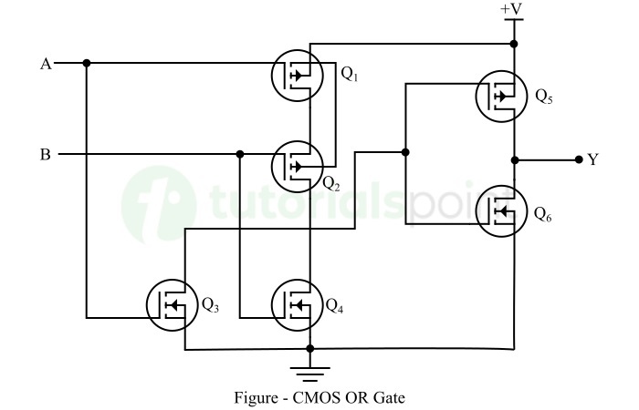
Here, we have combined multiple CMOS inverters together to build a CMOS OR gate. In the circuit diagram, the CMOS OR gate consists of a PMOS transistor and an NMOS transistor, which are joined in parallel fashion between the power supply voltage (V) and the output.
In the above circuit, when one or both inputs (A and B) are high (logic 1), the corresponding PMOS and NMOS transistors switch in a way that the current flows from the output to ground, causes a low voltage (logic 0) at the output terminal.
When both inputs are low (logic 0), the corresponding CMOS transistors switch in a way that the output is connected to the supply voltage, causing a high voltage (logic 1) at the output terminal.
CMOS AND Gate
The AND gate is a basic logic gate used in a variety of digital logic circuits. AND gate produces a high or logic 1 output only when all of its inputs are high, it produces a low or logic 0 output when any of its inputs is low.
The truth table of the two-input AND gate is given below.
| Input | Output | |
|---|---|---|
| A | B | Y = AB |
| 0 | 0 | 0 |
| 0 | 1 | 0 |
| 1 | 0 | 0 |
| 1 | 1 | 1 |
The implementation of AND gate using CMOS technology is shown in the following figure.
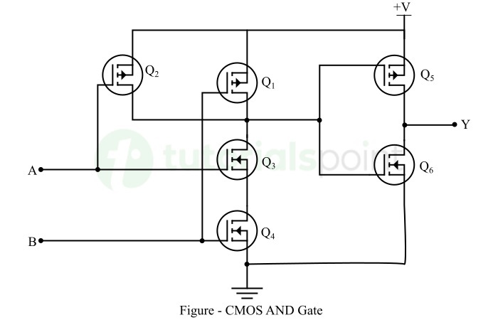
Here, to implement the CMOS AND gate, we have connected multiple CMOS inverters together. In the CMOS AND gate circuit, PMOS and NMOS transistors are used to build it. These transistors are connected in series between supply voltage (V) and the output (Y), and in parallel between the output and ground respectively.
In the case of CMOS AND gate shown in the above figure, when both inputs are high (logic 1), the CMOS transistors switch in such a way that the output is connected to the power supply voltage (V), producing a high (logic 1) output.
When any of its inputs is low, the CMOS transistors in the circuit switch such that the current flows from power supply to the ground, making output low (logic 0).
CMOS NOT Gate
A NOT gate is also a basic logic gate used in digital logic circuits. The NOT has a single input and a single output. The output of the NOT gate is high or logic 1 when its input is low or logic 0, and its output is low or logic 0 when its input is high or logic 1.
In CMOS logic gates, the CMOS NOT gate is the simplest CMOS logic gate. It is also called CMOS Inverter Gate.
The truth table of the NOT gate is given below.
| Input | Output |
|---|---|
| A | Y = A' |
| 0 | 1 |
| 1 | 0 |
The implementation of a NOT gate in CMOS technology is shown in the following figure.
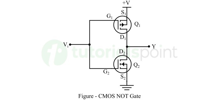
Here, the input is applied to the gate terminal of the two CMOS transistor, and the output is connected to their drain terminals.
When a positive voltage pulse (logic 1) is applied to the input Vi, the CMOS transistor Q1 is off and the CMOS transistor Q2 is on. Therefore, the output voltage will be at ground voltage, i.e. logic 0.
When the ground voltage (logic 0) is applied to the input Vi, the CMOS transistor Q1 is on and the CMOS transistor Q2 is off. Thus, the output will be closed to +V, i.e. logic 1.