- Digital Electronics - Home
- Digital Electronics Basics
- Types of Digital Systems
- Types of Signals
- Logic Levels And Pulse Waveforms
- Digital System Components
- Digital Logic Operations
- Digital Systems Advantages
- Number Systems
- Number Systems
- Binary Numbers Representation
- Binary Arithmetic
- Signed Binary Arithmetic
- Octal Arithmetic
- Hexadecimal Arithmetic
- Complement Arithmetic
- Base Conversions
- Base Conversions
- Binary to Decimal Conversion
- Decimal to Binary Conversion
- Binary to Octal Conversion
- Octal to Binary Conversion
- Octal to Decimal Conversion
- Decimal to Octal Conversion
- Hexadecimal to Binary Conversion
- Binary to Hexadecimal Conversion
- Hexadecimal to Decimal Conversion
- Decimal to Hexadecimal Conversion
- Octal to Hexadecimal Conversion
- Hexadecimal to Octal Conversion
- Binary Codes
- Binary Codes
- 8421 BCD Code
- Excess-3 Code
- Gray Code
- ASCII Codes
- EBCDIC Code
- Code Conversion
- Error Detection & Correction Codes
- Logic Gates
- Logic Gates
- AND Gate
- OR Gate
- NOT Gate
- Universal Gates
- XOR Gate
- XNOR Gate
- CMOS Logic Gate
- OR Gate Using Diode Resistor Logic
- AND Gate vs OR Gate
- Two Level Logic Realization
- Threshold Logic
- Boolean Algebra
- Boolean Algebra
- Laws of Boolean Algebra
- Boolean Functions
- DeMorgan's Theorem
- SOP and POS Form
- POS to Standard POS Form
- Minimization Techniques
- K-Map Minimization
- Three Variable K-Map
- Four Variable K-Map
- Five Variable K-Map
- Six Variable K-Map
- Don't Care Condition
- Quine-McCluskey Method
- Min Terms and Max Terms
- Canonical and Standard Form
- Max Term Representation
- Simplification using Boolean Algebra
- Combinational Logic Circuits
- Digital Combinational Circuits
- Digital Arithmetic Circuits
- Multiplexers
- Multiplexer Design Procedure
- Mux Universal Gate
- 2-Variable Function Using 4:1 Mux
- 3-Variable Function Using 8:1 Mux
- Demultiplexers
- Mux vs Demux
- Parity Bit Generator and Checker
- Comparators
- Encoders
- Keyboard Encoders
- Priority Encoders
- Decoders
- Arithmetic Logic Unit
- 7-Segment LED Display
- Code Converters
- Code Converters
- Binary to Decimal Converter
- Decimal to BCD Converter
- BCD to Decimal Converter
- Binary to Gray Code Converter
- Gray Code to Binary Converter
- BCD to Excess-3 Converter
- Excess-3 to BCD Converter
- Adders
- Half Adders
- Full Adders
- Serial Adders
- Parallel Adders
- Full Adder using Half Adder
- Half Adder vs Full Adder
- Full Adder with NAND Gates
- Half Adder with NAND Gates
- Binary Adder-Subtractor
- Subtractors
- Half Subtractors
- Full Subtractors
- Parallel Subtractors
- Full Subtractor using 2 Half Subtractors
- Half Subtractor using NAND Gates
- Sequential Logic Circuits
- Digital Sequential Circuits
- Clock Signal and Triggering
- Latches
- Shift Registers
- Shift Register Applications
- Binary Registers
- Bidirectional Shift Register
- Counters
- Binary Counters
- Non-binary Counter
- Design of Synchronous Counter
- Synchronous vs Asynchronous Counter
- Finite State Machines
- Algorithmic State Machines
- Flip Flops
- Flip-Flops
- Conversion of Flip-Flops
- D Flip-Flops
- JK Flip-Flops
- T Flip-Flops
- SR Flip-Flops
- Clocked SR Flip-Flop
- Unclocked SR Flip-Flop
- Clocked JK Flip-Flop
- JK to T Flip-Flop
- SR to JK Flip-Flop
- Triggering Methods:Flip-Flop
- Edge-Triggered Flip-Flop
- Master-Slave JK Flip-Flop
- Race-around Condition
- A/D and D/A Converters
- Analog-to-Digital Converter
- Digital-to-Analog Converter
- DAC and ADC ICs
- Realization of Logic Gates
- NOT Gate from NAND Gate
- OR Gate from NAND Gate
- AND Gate from NAND Gate
- NOR Gate from NAND Gate
- XOR Gate from NAND Gate
- XNOR Gate from NAND Gate
- NOT Gate from NOR Gate
- OR Gate from NOR Gate
- AND Gate from NOR Gate
- NAND Gate from NOR Gate
- XOR Gate from NOR Gate
- XNOR Gate from NOR Gate
- NAND/NOR Gate using CMOS
- Full Subtractor using NAND Gate
- AND Gate Using 2:1 MUX
- OR Gate Using 2:1 MUX
- NOT Gate Using 2:1 MUX
- Memory Devices
- Memory Devices
- RAM and ROM
- Cache Memory Design
- Programmable Logic Devices
- Programmable Logic Devices
- Programmable Logic Array
- Programmable Array Logic
- Field Programmable Gate Arrays
- Digital Electronics Families
- Digital Electronics Families
- CPU Architecture
- CPU Architecture
Implementation of NAND/NOR gate using CMOS
In digital electronics, NAND and NOR gates are two universal logic gates that are used to perform Boolean operations on multiple input variables. These gates produce an output based on the combination of inputs applied.
NAND and NOR gates are used as the fundamental building blocks in the digital circuits and systems. We can design and implement the NAND and NOR gates in different technologies such as DTL, RTL, TTL, and CMOS. This chapter deals with implementation of NAND and NOR gates using CMOS technology.
In CMOS (Complementary Metal Oxide Semiconductor) technology, the NAND and NOR logic gates are designed by connecting NMOS and PMOS transistors in series and parallel connections. The block diagram of a 2-input logic gate in CMOS technology is shown in the following figure.
Before getting deeper into the NAND and NOR gate using CMOS technology. Lets first study the basics of NAND and NOR gates individually.
NAND Gate
The NAND gate is a combination of NOT gate and AND gate, where a NOT gate connected to the output of the AND gate. Thus, it is also known as NOTed AND gate.
$$\mathrm{AND \: Gate \: + \: NOT \: Gate \: = \: NAND \: Gate}$$
The logic circuit symbol of a two input NAND gate is shown in the following figure −
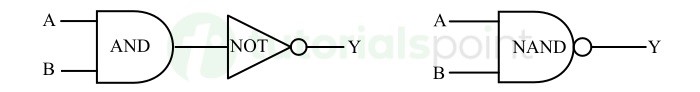
The NAND gate produces a low or logic 0 output when all inputs applied to it are high or logic 1. For all other input combinations, it produces a high or logic 1 output.
Truth Table of NAND Gate
The truth table of a two input NAND gate is shown here −
| Inputs | Output | |
|---|---|---|
| A | B | Y |
| 0 | 0 | 1 |
| 0 | 1 | 1 |
| 1 | 0 | 1 |
| 1 | 1 | 0 |
From this truth table, we can write the Boolean expression of the NAND gate, as follows.
$$\mathrm{Y \: = \: \overline{A\cdot B}}$$
Here, Y is the output variable, and A and B are the input variables.
NOR Gate
The NOR gate is a universal logic gate in digital electronics. It is a combination of two basic logic gates namely, NOT gate and OR gate, where it is realized by connecting a NOT gate to the output of the OR gate. Therefore,
$$\mathrm{OR \: Gate \: + \: NOT \: Gate \: = \: NOR \: Gate}$$
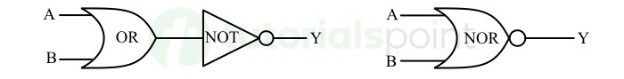
The output of the NOR gate is high or logic 1, when all its inputs are low or logic 0. For all other input combinations, the output of the NOR gate is low or logic 0.
Truth Table of NOR Gate
The following is the truth table of a two input NOR gate that describing its operation −
| Inputs | Output | |
|---|---|---|
| A | B | Y |
| 0 | 0 | 1 |
| 0 | 1 | 0 |
| 1 | 0 | 0 |
| 1 | 1 | 0 |
From this truth table, we can write the Boolean expression of the NOR gate, as follows.
$$\mathrm{Y \: = \: \overline{A \: + \: B}}$$
Here, Y is the output variable, and A and B are the input variables.
This is all about the basics of NAND and NOR gate. Let us now discuss the implementation of NAND and NOR gates using CMOS technology.
NAND Gate Using CMOS Technology
The NAND gate can be implemented in CMOS technology by using PMOS and NMOS transistors. The circuit diagram of a two input NAND gate in CMOS technology is shown in the following figure −
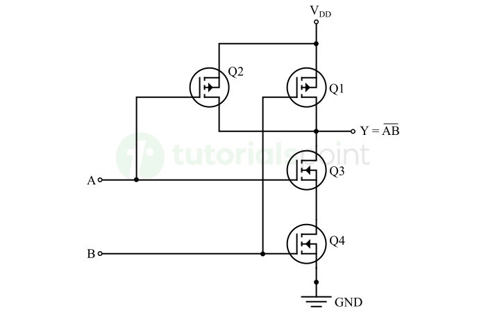
It consists of two PMOS transistors Q1 and Q2 and two NMOS transistors Q3 and Q4. The PMOS transistors are connected in parallel between the power supply VDD and the output terminal Y. Similarly, the NMOS transistors are connected in series between the output terminal Y and the ground terminal GND.
Now, let us understand the operation of this CMOS NAND gate.
Case 1: When Input A is Low and Input B is Low
In this case, when both inputs A and B are low, the PMOS transistors Q1 and Q2 are ON and the NMOS transistors Q3 and Q4 are OFF. Hence, there is a closed path between the supply voltage VDD and the output terminal Y.
Thus, the output Y will be connected to the voltage level VDD. Also, there is no path between the output terminal and the ground terminal as both NMOS transistors are OFF. Under this condition, the output line will maintain the voltage level at VDD, which indicates the output High.
Thus, when A = 0 and B = 0, then Y = 1
Case 2: When Input A is Low and Input B is High
In this case, the PMOS transistor Q1 will be ON while the PMOS transistor Q2 will be OFF. The NMOS transistor Q3 will be OFF and the NMOS transistor Q4 will be ON.
For this switching condition of the CMOS transistors, the power supply VDD will get a path to the output terminal through the PMOS transistor Q1. Since, the NMOS transistor Q3 and Q4 are connected in series and the NMOS transistor Q3 is OFF. Hence, there is no path between the output terminal and the ground terminal.
Therefore, the output terminal Y maintain the voltage level at VDD and results in a High output.
Thus, when A = 0 and B = 1, then Y = 1
Case 3: When Input A is High and Input B is Low
In this case, the PMOS transistor Q1 will be OFF and the PMOS transistor Q2 will be ON. The NMOS transistor Q3 will be ON and the NMOS transistor Q4 will be OFF.
Under this switching condition of the CMOS transistors, the output terminal will connect to the power supply through the PMOS transistor Q2. Since, both NMOS transistors are connected in series and the NMOS transistor Q4 is OFF. Hence, there is no path between the output terminal and the ground terminal.
Therefore, the output line will maintain the voltage level at VDD and results in a High output.
Thus, when A = 1 and B = 0, then Y = 1
Case 4: When Input A is High and Input B is High
In this case, both PMOS transistors Q1 and Q2 will be OFF and both NMOS transistors will be ON. In this case, there is no path between the output terminal and the power supply VDD, but there is a direct path between the output terminal and the ground terminal. This results in a ground voltage level at the output terminal and produces a Low output.
Hence, when A = 1 and B = 1, then Y = 0
The operation of this CMOS NAND gate is shown in the following truth table −
| Inputs | Output | |
|---|---|---|
| A | B | Y |
| Low (0) | Low (0) | High (1) |
| Low (0) | High (1) | High (1) |
| High (1) | Low (0) | High (1) |
| High (1) | High (1) | Low (0) |
This is all about NAND gate implementation using CMOS technology and its operation for different input combinations.
Let us now discuss the implementation and operation of NOR gate using CMOS technology.
NOR Gate Using CMOS Technology
Similar to CMOS NAND gate, we can also design a NOR gate using PMOS and NMOS transistors. The circuit diagram of a two input NOR gate using CMOS technology is shown in the following figure −
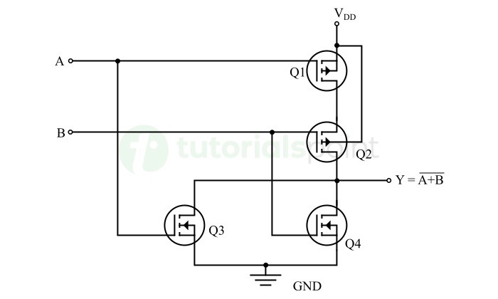
This CMOS NOR gate is designed by using two PMOS transistors Q1 and Q2 and two NMOS transistor Q3 and Q4. Where the PMOS transistors are connected in series between the supply voltage VDD and the output terminal Y. The NMOS transistors are connected in parallel between the output terminal Y and the ground terminal GND.
Now, let us understand how does this CMOS circuit operate as a two input NOR gate.
Case 1: When Input A is Low and Input B is Low
In this case, both PMOS transistors Q1 and Q2 will be ON and both NMOS transistors Q3 and Q4 will be OFF.
Under this switching condition of the CMOS transistors, there is a path between the supply voltage VDD and the output terminal Y through the ON PMOS transistors. But there is no path between the output terminal Y and the ground terminal GND. This maintains the output at the voltage level VDD and hence the output will be High.
Thus, when A = 0 and B = 0, then Y = 1
Case 2: When Input A is Low and Input B is High
In this case, the PMOS transistor Q1 is ON, the PMOS transistor Q2 is OFF, the NMOS transistor Q3 is OFF, and the NMOS transistor Q4 is ON.
Since, the PMOS transistors Q1 and Q2 are connected in series and the transistor Q2 is OFF. Thus, there is no path between the power supply VDD and the output terminal Y. But there is a connection between the output line Y and the ground terminal GND through the ON NMOS transistor Q4. This sets the output terminal to ground voltage and makes the output Low.
Therefore, when A = 0 and B = 1, then Y = 0
Case 3: When Input A is High and Input B is Low
In this condition, the PMOS transistor Q1 is OFF, the PMOS transistor Q2 is ON, the NMOS transistor Q3 is ON, and the NMOS transistor Q4 is OFF.
In this case, there is no closed path between the power supply VDD and the output line Y due to OFF PMOS transistor Q1. But there is a closed between the output line Y and the ground terminal GND through the ON NMOS transistor Q3. Hence, the output terminal is connected to the ground potential and makes the output Low.
Thus, when A = 1 and B = 0, then Y = 0
Case 4 When Input A is High and Input B is High
In this case, both PMOS transistors Q1 and Q2 are OFF and both NMOS transistors Q3 and Q4 are ON. Under this condition, there is no path between the supply voltage VDD and the output terminal Y. But there is a closed path between the output terminal Y and the ground terminal GND. This maintains the output line at ground voltage level and hence the output will be Low.
Thus, when A = 1 and B = 1, then Y = 0
This complete operation of the CMOS NOR gate can be summarized in the form of a truth table which is given below.
| Inputs | Output | |
|---|---|---|
| A | B | Y |
| Low (0) | Low (0) | High (1) |
| Low (0) | High (1) | Low (0) |
| High (1) | Low (0) | Low (0) |
| High (1) | High (1) | Low (0) |
Advantages of NAND and NOR Gates using CMOS Technology
NAND and NOR gates implemented in CMOS technology offer several benefits over other technologies. Some of the key advantages of CMOS NAND and NOR gates are listed here −
- CMOS NAND and NOR gates consume relatively low power. This advantage makes these logic gates well-suited to use in battery powered devices.
- NAND and NOR gates designed using CMOS technology have high immunity against noise and interference. They can be designed to have a wider range of operating voltage.
- The CMOS technology offers high-density integration that allows for implementing a large number of NAND and NOR gates on a single chip. These gates provide symmetrical output characteristics that allow them to integrate with different types of digital circuits seamlessly.
- CMOS technology is one of the well-established, mature, and cost-effective semiconductor manufacturing technology. Hence, the CMOS NAND and NOR gates are relatively easy to manufacture and cost effective.
Applications of CMOS NAND and NOR Gates
The CMOS NAND and NOR gates are widely used in the following applications due to their benefits and versatility −
- CMOS NAND and NOR gates are widely used in the logic circuit designs to perform logical operations.
- In digital systems, the CMOS NAND and NOR gates are used to implement arithmetic circuits like adders, subtractors, multipliers, etc.
- They are also used in memory units to implement memory cell structures.
- CMOS NAND and NOR gates are also used to design multiplexers and demultiplexers.
- Some other common applications of CMOS NAND and NOR gates include digital signal processing, digital timing circuits, analog to digital conversion, digital communication, etc.
Conclusion
The CMOS NAND and NOR gates are widely used in a variety of applications in the field of digital electronics. This type of NAND and NOR gates offer several advantages such as high efficiency, low power consumption, versatility, low cost, high reliability, etc.
In this chapter, we explained the implementation of NAND and NOR gates using CMOS technology along with their advantages and applications.