- Digital Electronics - Home
- Digital Electronics Basics
- Types of Digital Systems
- Types of Signals
- Logic Levels And Pulse Waveforms
- Digital System Components
- Digital Logic Operations
- Digital Systems Advantages
- Number Systems
- Number Systems
- Binary Numbers Representation
- Binary Arithmetic
- Signed Binary Arithmetic
- Octal Arithmetic
- Hexadecimal Arithmetic
- Complement Arithmetic
- Base Conversions
- Base Conversions
- Binary to Decimal Conversion
- Decimal to Binary Conversion
- Binary to Octal Conversion
- Octal to Binary Conversion
- Octal to Decimal Conversion
- Decimal to Octal Conversion
- Hexadecimal to Binary Conversion
- Binary to Hexadecimal Conversion
- Hexadecimal to Decimal Conversion
- Decimal to Hexadecimal Conversion
- Octal to Hexadecimal Conversion
- Hexadecimal to Octal Conversion
- Binary Codes
- Binary Codes
- 8421 BCD Code
- Excess-3 Code
- Gray Code
- ASCII Codes
- EBCDIC Code
- Code Conversion
- Error Detection & Correction Codes
- Logic Gates
- Logic Gates
- AND Gate
- OR Gate
- NOT Gate
- Universal Gates
- XOR Gate
- XNOR Gate
- CMOS Logic Gate
- OR Gate Using Diode Resistor Logic
- AND Gate vs OR Gate
- Two Level Logic Realization
- Threshold Logic
- Boolean Algebra
- Boolean Algebra
- Laws of Boolean Algebra
- Boolean Functions
- DeMorgan's Theorem
- SOP and POS Form
- POS to Standard POS Form
- Minimization Techniques
- K-Map Minimization
- Three Variable K-Map
- Four Variable K-Map
- Five Variable K-Map
- Six Variable K-Map
- Don't Care Condition
- Quine-McCluskey Method
- Min Terms and Max Terms
- Canonical and Standard Form
- Max Term Representation
- Simplification using Boolean Algebra
- Combinational Logic Circuits
- Digital Combinational Circuits
- Digital Arithmetic Circuits
- Multiplexers
- Multiplexer Design Procedure
- Mux Universal Gate
- 2-Variable Function Using 4:1 Mux
- 3-Variable Function Using 8:1 Mux
- Demultiplexers
- Mux vs Demux
- Parity Bit Generator and Checker
- Comparators
- Encoders
- Keyboard Encoders
- Priority Encoders
- Decoders
- Arithmetic Logic Unit
- 7-Segment LED Display
- Code Converters
- Code Converters
- Binary to Decimal Converter
- Decimal to BCD Converter
- BCD to Decimal Converter
- Binary to Gray Code Converter
- Gray Code to Binary Converter
- BCD to Excess-3 Converter
- Excess-3 to BCD Converter
- Adders
- Half Adders
- Full Adders
- Serial Adders
- Parallel Adders
- Full Adder using Half Adder
- Half Adder vs Full Adder
- Full Adder with NAND Gates
- Half Adder with NAND Gates
- Binary Adder-Subtractor
- Subtractors
- Half Subtractors
- Full Subtractors
- Parallel Subtractors
- Full Subtractor using 2 Half Subtractors
- Half Subtractor using NAND Gates
- Sequential Logic Circuits
- Digital Sequential Circuits
- Clock Signal and Triggering
- Latches
- Shift Registers
- Shift Register Applications
- Binary Registers
- Bidirectional Shift Register
- Counters
- Binary Counters
- Non-binary Counter
- Design of Synchronous Counter
- Synchronous vs Asynchronous Counter
- Finite State Machines
- Algorithmic State Machines
- Flip Flops
- Flip-Flops
- Conversion of Flip-Flops
- D Flip-Flops
- JK Flip-Flops
- T Flip-Flops
- SR Flip-Flops
- Clocked SR Flip-Flop
- Unclocked SR Flip-Flop
- Clocked JK Flip-Flop
- JK to T Flip-Flop
- SR to JK Flip-Flop
- Triggering Methods:Flip-Flop
- Edge-Triggered Flip-Flop
- Master-Slave JK Flip-Flop
- Race-around Condition
- A/D and D/A Converters
- Analog-to-Digital Converter
- Digital-to-Analog Converter
- DAC and ADC ICs
- Realization of Logic Gates
- NOT Gate from NAND Gate
- OR Gate from NAND Gate
- AND Gate from NAND Gate
- NOR Gate from NAND Gate
- XOR Gate from NAND Gate
- XNOR Gate from NAND Gate
- NOT Gate from NOR Gate
- OR Gate from NOR Gate
- AND Gate from NOR Gate
- NAND Gate from NOR Gate
- XOR Gate from NOR Gate
- XNOR Gate from NOR Gate
- NAND/NOR Gate using CMOS
- Full Subtractor using NAND Gate
- AND Gate Using 2:1 MUX
- OR Gate Using 2:1 MUX
- NOT Gate Using 2:1 MUX
- Memory Devices
- Memory Devices
- RAM and ROM
- Cache Memory Design
- Programmable Logic Devices
- Programmable Logic Devices
- Programmable Logic Array
- Programmable Array Logic
- Field Programmable Gate Arrays
- Digital Electronics Families
- Digital Electronics Families
- CPU Architecture
- CPU Architecture
NOT Gate in Digital Electronics
The NOT gate is a type of basic logic gate having only one input line and one output line. It performs the inversion operation.
In this chapter, we will explain the theory of NOT gate, its logic symbol, working, truth table, Boolean expression, etc.
In digital electronics, the NOT gate is used as the basic building block of complex digital systems.
What is a NOT Gate?
The NOT gate is a type of basic logic gate used in digital electronics to implement the inversion function. Since it performs the inversion operation, it is also known as inverter.
It has only one input line and one output line. The output of the NOT gate is high or logic 1 when its input is low or logic 0. The output of the NOT gate is low or logic 0 when its input is high or logic 1.
The logic symbol of the NOT gate is shown in the following figure −

Here, A is the input line and Y is the output line of the NOT gate.
Truth Table of NOT Gate
The truth table of NOT gate is a table of input and output that represent the relationship between them. Here is the truth table of the NOT gate −
| Input (A) | Output (Y) |
|---|---|
| 0 | 1 |
| 1 | 0 |
From this truth table, we can observe that the NOT gate inverts the input applied to it. Hence, if we apply a high input, it produces a low output and vice-versa.
Boolean Expression of NOT Gate
The Boolean expression of the NOT gate is a logical function that explains the relationship between input and output of the NOT gate mathematically.
The Boolean expression of the NOT gate is given below −
$$\mathrm{Y \: = \: \bar{A} \: = \: A'}$$
Here, the symbols "(-) overbar" and "(') prime" represents the inversion or complement operation.
This expression is read as "Y is equal to A bar or A prime or NOTed A".
Working of NOT Gate
The NOT gate performs the inversion operation of the input applied. The complete working of the NOT gate for possible input combinations is explained below −
- If A = 0, the output is Y = 1.
- If A = 1, the output is Y = 0.
Thus, the output of the NOT gate is the complement of the input applied to it.
NOT Gate using Transistor
We can implement the NOT gate logic by using a BJT transistor. When the NOT gate is implemented using a transistor, it is called a transistor inverter.
The following figure shows the circuit diagram of a NOT gate using transistor or transistor inverter.
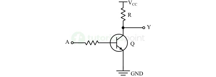
Working of Transistor NOT Gate
The above transistor inverter circuit operates as described below −
When the input A is low, the transistor will be inactive and acts as an open switch. Thus, there is no closed path between the power supply VCC and ground terminal. Hence, the total supply voltage will appear at the output line. This represents the high or logic 1 output.
When the input A is high, the transistor will turn on and act as a closed switch. As a result, the power supply is directly connected to the ground terminal and the voltage available at the output line is equal to the ground voltage. This makes the output of the circuit low or logic 0.
This is how, the above transistor circuit implements the NOT logic.
NOT Gate using Switches
We can also implement the NOT gate operation using a battery, a switch, and a lamp. The circuit diagram for the NOT gate using switches is shown in the following figure.

In this circuit, when the switch A is open, i.e., logic 0, the current follows the path through the lamp making it glow. This represents a high or logic 1 output.
If the switch A is closed, i.e., logic 1, the current flows through the short-circuited path provided by the closed switch and no current will flow through the lamp. Hence, in this case, the lamp will be off and represents the low or logic 0 output.
From this discussion, it is clear that the output is high when the input is low and vice-versa. Thus, the above switching circuit implements the NOT gate logic.
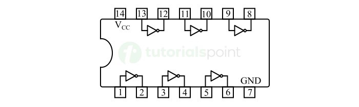
NOT Gate IC
The NOT gate comes in the form of integrated circuits or ICs. The most commonly used NOT gate IC is IC 7404. It contains six TL (transistor logic) NOT gates.
The pin diagram of the NOT gate IC 7404 is depicted in the following figure.
Applications of NOT Gate
The NOT gate is an essential building block of various digital systems and circuits. Some key applications of NOT gate are described below −
- NOT gate is used in inverters to convert a high signal to a low signal and a low signal to a high signal.
- NOT gate is used in communication systems and storage devices.
- NOT gate is also employed as interfacing device between different logic families.
- NOT gate is also used in various digital circuits like timers, oscillators, multivibrators, modulators, etc.
Conclusion
In conclusion, the NOT gate is a logic gate used in digital electronics to implement inversion operation. It has only one input line and one output line.
The output of the NOT gate is the complement of the input signal applied to it. In this chapter, we explained the basic theory of NOT gate along with its working and applications.