- Digital Electronics - Home
- Digital Electronics Basics
- Types of Digital Systems
- Types of Signals
- Logic Levels And Pulse Waveforms
- Digital System Components
- Digital Logic Operations
- Digital Systems Advantages
- Number Systems
- Number Systems
- Binary Numbers Representation
- Binary Arithmetic
- Signed Binary Arithmetic
- Octal Arithmetic
- Hexadecimal Arithmetic
- Complement Arithmetic
- Base Conversions
- Base Conversions
- Binary to Decimal Conversion
- Decimal to Binary Conversion
- Binary to Octal Conversion
- Octal to Binary Conversion
- Octal to Decimal Conversion
- Decimal to Octal Conversion
- Hexadecimal to Binary Conversion
- Binary to Hexadecimal Conversion
- Hexadecimal to Decimal Conversion
- Decimal to Hexadecimal Conversion
- Octal to Hexadecimal Conversion
- Hexadecimal to Octal Conversion
- Binary Codes
- Binary Codes
- 8421 BCD Code
- Excess-3 Code
- Gray Code
- ASCII Codes
- EBCDIC Code
- Code Conversion
- Error Detection & Correction Codes
- Logic Gates
- Logic Gates
- AND Gate
- OR Gate
- NOT Gate
- Universal Gates
- XOR Gate
- XNOR Gate
- CMOS Logic Gate
- OR Gate Using Diode Resistor Logic
- AND Gate vs OR Gate
- Two Level Logic Realization
- Threshold Logic
- Boolean Algebra
- Boolean Algebra
- Laws of Boolean Algebra
- Boolean Functions
- DeMorgan's Theorem
- SOP and POS Form
- POS to Standard POS Form
- Minimization Techniques
- K-Map Minimization
- Three Variable K-Map
- Four Variable K-Map
- Five Variable K-Map
- Six Variable K-Map
- Don't Care Condition
- Quine-McCluskey Method
- Min Terms and Max Terms
- Canonical and Standard Form
- Max Term Representation
- Simplification using Boolean Algebra
- Combinational Logic Circuits
- Digital Combinational Circuits
- Digital Arithmetic Circuits
- Multiplexers
- Multiplexer Design Procedure
- Mux Universal Gate
- 2-Variable Function Using 4:1 Mux
- 3-Variable Function Using 8:1 Mux
- Demultiplexers
- Mux vs Demux
- Parity Bit Generator and Checker
- Comparators
- Encoders
- Keyboard Encoders
- Priority Encoders
- Decoders
- Arithmetic Logic Unit
- 7-Segment LED Display
- Code Converters
- Code Converters
- Binary to Decimal Converter
- Decimal to BCD Converter
- BCD to Decimal Converter
- Binary to Gray Code Converter
- Gray Code to Binary Converter
- BCD to Excess-3 Converter
- Excess-3 to BCD Converter
- Adders
- Half Adders
- Full Adders
- Serial Adders
- Parallel Adders
- Full Adder using Half Adder
- Half Adder vs Full Adder
- Full Adder with NAND Gates
- Half Adder with NAND Gates
- Binary Adder-Subtractor
- Subtractors
- Half Subtractors
- Full Subtractors
- Parallel Subtractors
- Full Subtractor using 2 Half Subtractors
- Half Subtractor using NAND Gates
- Sequential Logic Circuits
- Digital Sequential Circuits
- Clock Signal and Triggering
- Latches
- Shift Registers
- Shift Register Applications
- Binary Registers
- Bidirectional Shift Register
- Counters
- Binary Counters
- Non-binary Counter
- Design of Synchronous Counter
- Synchronous vs Asynchronous Counter
- Finite State Machines
- Algorithmic State Machines
- Flip Flops
- Flip-Flops
- Conversion of Flip-Flops
- D Flip-Flops
- JK Flip-Flops
- T Flip-Flops
- SR Flip-Flops
- Clocked SR Flip-Flop
- Unclocked SR Flip-Flop
- Clocked JK Flip-Flop
- JK to T Flip-Flop
- SR to JK Flip-Flop
- Triggering Methods:Flip-Flop
- Edge-Triggered Flip-Flop
- Master-Slave JK Flip-Flop
- Race-around Condition
- A/D and D/A Converters
- Analog-to-Digital Converter
- Digital-to-Analog Converter
- DAC and ADC ICs
- Realization of Logic Gates
- NOT Gate from NAND Gate
- OR Gate from NAND Gate
- AND Gate from NAND Gate
- NOR Gate from NAND Gate
- XOR Gate from NAND Gate
- XNOR Gate from NAND Gate
- NOT Gate from NOR Gate
- OR Gate from NOR Gate
- AND Gate from NOR Gate
- NAND Gate from NOR Gate
- XOR Gate from NOR Gate
- XNOR Gate from NOR Gate
- NAND/NOR Gate using CMOS
- Full Subtractor using NAND Gate
- AND Gate Using 2:1 MUX
- OR Gate Using 2:1 MUX
- NOT Gate Using 2:1 MUX
- Memory Devices
- Memory Devices
- RAM and ROM
- Cache Memory Design
- Programmable Logic Devices
- Programmable Logic Devices
- Programmable Logic Array
- Programmable Array Logic
- Field Programmable Gate Arrays
- Digital Electronics Families
- Digital Electronics Families
- CPU Architecture
- CPU Architecture
Programmable Logic Array (PLA)
In this chapter, we will talk about Programmable Logic Array (PLA), its block diagram, and applications. The programmable logic array (PLA) is a type of programmable logic device (PLD). Historically, PLA is the first PLD device. It contains an array/matrix of AND and OR gates whose configuration is done as per the needs of applications.
In a PLA, a set of fusible links is used to establish or remove the contact of a literal in the AND operation or contact of a product term in the OR operation. Therefore, a PLA is a type of PLD that allows both AND matrix and OR matrix to program.
In digital electronics, PLAs are used to design and implement a variety of complex combinational circuits. However, some PLAs also have a memory element, hence they can be used to implement sequential circuits as well.
Block Diagram of PLA
A programmable logic array (PLA) is a type of fixed architecture programmable logic device (PLD) which consists of programmable AND and OR gates. A PLA contains a programmable AND array which is followed by a programmable OR array.
The block diagram of the PLA is shown in the following figure −
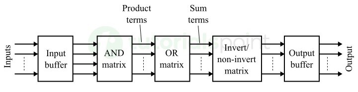
It consists of the following main components −
Input Buffer
The input buffer is used in PLA to avoid the loading effect on the source that drives the inputs.
AND Array/Matrix
The AND array/matrix is used in PLA to generate the product terms.
OR Array/Matrix
In a PLA, the OR array/matrix is used to generate the desired output. This is done by Oring the product terms to produce the sum terms.
Invert/Non-Invert Matrix
It is a buffer used in PLAs to set the output to active-high or active-low.
Output Buffer
This buffer is used at the output side. It is mainly provided to increase the driving capability of the programmable logic array (PLA).
Combinational Logic Design using PLA
In the field of digital electronics, the PLAs are extensively used for designing combinational logic circuits. The greatest advantage of designing combinational circuits using PLAs is that PLA consist of programmable AND and OR arrays which allows to implement custom desired logic functions.
The step-by-step procedure to design a combinational logic circuit using PLAs is explained below −
Step 1 − Develop a PLA program table that shows the inputs, product terms, and outputs.
Step 2 − Design the AND matrix that can generate the desired product terms.
Step 3 − Design the OR matrix that can generate the desired output.
Step 4 − Design the invert/non-invert matrix to set the active-low or active-high output.
Step 5 − Finally, program the PLA by utilizing the PLA program table.
Let us understand this process of combinational circuit design using PLA with the help of an example.
Example
Design a full-adder circuit using programmable logic array (PLA).
Solution
A full-adder consists of three-inputs and two outputs. Since it has 3 inputs, thus there are total 8 product terms which are given in the following truth table of the full adder −
| Inputs | Outputs | |||
|---|---|---|---|---|
| A | B | Cin | S | Cout |
| 0 | 0 | 0 | 0 | 0 |
| 0 | 0 | 1 | 1 | 0 |
| 0 | 1 | 0 | 1 | 0 |
| 0 | 1 | 1 | 0 | 1 |
| 1 | 0 | 0 | 1 | 0 |
| 1 | 0 | 1 | 0 | 1 |
| 1 | 1 | 0 | 0 | 1 |
| 1 | 1 | 1 | 1 | 1 |
From this truth table, the output sum (S) and the output carry (Cout) are given by,
$$\mathrm{S \: = \: \sum \: m(1,2,4,7)}$$
$$\mathrm{C_{out} \: = \: \sum \: m(3,5,6,7)}$$
Thus, their Boolean expressions will be,
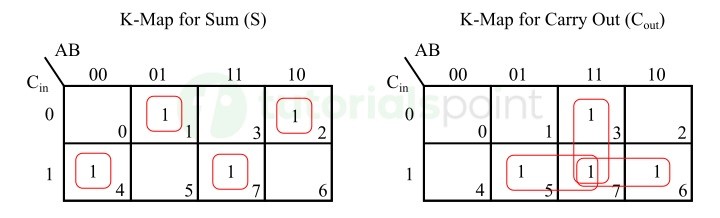
$$\mathrm{S \: = \: \overline{A} \: B \: \overline{C_{in}} \: + \: \overline{A} \: \overline{B} \: C_{in} \: + \: A \: \overline{B} \: \overline{C_{in}} \: + \: A \: B \: C_{in}}$$
$$\mathrm{C_{out} \: = \: A \: B \: + \: B \: C_{in} \: + \: A \: C_{in}}$$
From these two Boolean expressions, we can see that there are seven product terms and two sum terms. The PLA program table for this full-adder circuit is shown below −
| Sr.No | Product Terms | Inputs | Outputs | |||
|---|---|---|---|---|---|---|
| A | B | Cin | S | Cout | ||
| 1 | $\mathrm{\overline{A} \: B \: \overline{C_{in}}}$ | 0 | 1 | 0 | 1 | - |
| 2 | $\mathrm{\overline{A} \: \overline{B} \: C_{in}}$ | 0 | 0 | 1 | 1 | - |
| 3 | $\mathrm{A \: \overline{B} \: \overline{C_{in}}}$ | 1 | 0 | 0 | 1 | - |
| 4 | $\mathrm{A \: B \: C_{in}}$ | 1 | 1 | 1 | 1 | - |
| 5 | $\mathrm{A \: B }$ | 1 | 1 | - | - | 1 |
| 6 | $\mathrm{B \: C_{in}}$ | - | 1 | 1 | - | 1 |
| 7 | $\mathrm{A \: C_{in}}$ | 1 | - | 1 | - | 1 |
| T | T | |||||
In this PLA program table, "1" stands for the connection and "-" stands for the absence of the product term in the output. "T" stands for true and it represents the active-high output.
The PLA circuit diagram of the full-adder is shown in the following figure.
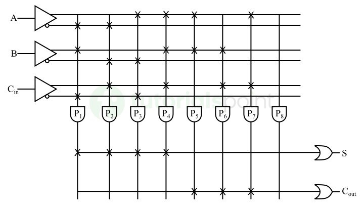
This example illustrates the complete step-by-step procedure to implement a combinational logic circuit using PLA.
Advantages of PLAs
The following are some key advantages of Programmable Logic Arrays (PLAs) that make them indispensable in the field of digital electronics −
- PLAs provide flexibility in terms of design and implementation of a variety of digital logic operations. PLAs can be used to implement custom logic functions required to fulfil the needs of different applications.
- PLAs also minimize the time required to design and develop a new digital circuit or system.
- PLAs provide a less expensive way of implementing highly complex digital logic functions. PLAs eliminate the need of discrete components to implement a logic function, hence they result in space efficiency.
- Since PLAs are programmable, they can be modified on their designs without re-fabricating the entire circuit.
Disadvantages of PLAs
However, PLAs offer several advantages as discussed above. But they also have some disadvantages which are listed below −
- For a large number of inputs and outputs, PLAs are highly complex to design and implement. Being a fixed architecture device, PLAs have limited performance in terms of speed and processing power.
- A PLA is generally optimized for a specific application, as it has a fixed number of AND gates and OR gates. This constraint disallows the designers to implement highly complex logic functions with the same PLA.
- Program a PLA is a time consuming and complex process.
Applications of PLAs
Programmable Logic Arrays (PLAs) are widely used in various applications across different fields. The following are some common applications of PLAs −
- PLAs are used in the field of digital signal processing to implement various logical functions, such as filtering, convolution, Fourier transformation, etc.
- In control systems, PLAs are used to implement control logic functions of various components like feedback, PID controllers, state machines, etc.
- PLAs are used to perform different types of arithmetic operations like addition, subtraction, multiplication, and division.
- PLAs also find their application in the field data compression and encryption technologies. PLAs are used in digital communication systems and networking equipment to implement algorithms for protocol handling, packet processing, error detection and correction, and more.
- PLAs are also used in different measuring instruments such as digital oscilloscopes, protocol analyzers, logic analyzer, etc.
Conclusion
A PLA is nothing but a kind of digital logic device used to implement complex digital functions without need of discrete components like AND gates, OR gates, etc. In this chapter, we explained the basics and applications of programmable logic arrays (PLAs).