- Digital Electronics - Home
- Digital Electronics Basics
- Types of Digital Systems
- Types of Signals
- Logic Levels And Pulse Waveforms
- Digital System Components
- Digital Logic Operations
- Digital Systems Advantages
- Number Systems
- Number Systems
- Binary Numbers Representation
- Binary Arithmetic
- Signed Binary Arithmetic
- Octal Arithmetic
- Hexadecimal Arithmetic
- Complement Arithmetic
- Base Conversions
- Base Conversions
- Binary to Decimal Conversion
- Decimal to Binary Conversion
- Binary to Octal Conversion
- Octal to Binary Conversion
- Octal to Decimal Conversion
- Decimal to Octal Conversion
- Hexadecimal to Binary Conversion
- Binary to Hexadecimal Conversion
- Hexadecimal to Decimal Conversion
- Decimal to Hexadecimal Conversion
- Octal to Hexadecimal Conversion
- Hexadecimal to Octal Conversion
- Binary Codes
- Binary Codes
- 8421 BCD Code
- Excess-3 Code
- Gray Code
- ASCII Codes
- EBCDIC Code
- Code Conversion
- Error Detection & Correction Codes
- Logic Gates
- Logic Gates
- AND Gate
- OR Gate
- NOT Gate
- Universal Gates
- XOR Gate
- XNOR Gate
- CMOS Logic Gate
- OR Gate Using Diode Resistor Logic
- AND Gate vs OR Gate
- Two Level Logic Realization
- Threshold Logic
- Boolean Algebra
- Boolean Algebra
- Laws of Boolean Algebra
- Boolean Functions
- DeMorgan's Theorem
- SOP and POS Form
- POS to Standard POS Form
- Minimization Techniques
- K-Map Minimization
- Three Variable K-Map
- Four Variable K-Map
- Five Variable K-Map
- Six Variable K-Map
- Don't Care Condition
- Quine-McCluskey Method
- Min Terms and Max Terms
- Canonical and Standard Form
- Max Term Representation
- Simplification using Boolean Algebra
- Combinational Logic Circuits
- Digital Combinational Circuits
- Digital Arithmetic Circuits
- Multiplexers
- Multiplexer Design Procedure
- Mux Universal Gate
- 2-Variable Function Using 4:1 Mux
- 3-Variable Function Using 8:1 Mux
- Demultiplexers
- Mux vs Demux
- Parity Bit Generator and Checker
- Comparators
- Encoders
- Keyboard Encoders
- Priority Encoders
- Decoders
- Arithmetic Logic Unit
- 7-Segment LED Display
- Code Converters
- Code Converters
- Binary to Decimal Converter
- Decimal to BCD Converter
- BCD to Decimal Converter
- Binary to Gray Code Converter
- Gray Code to Binary Converter
- BCD to Excess-3 Converter
- Excess-3 to BCD Converter
- Adders
- Half Adders
- Full Adders
- Serial Adders
- Parallel Adders
- Full Adder using Half Adder
- Half Adder vs Full Adder
- Full Adder with NAND Gates
- Half Adder with NAND Gates
- Binary Adder-Subtractor
- Subtractors
- Half Subtractors
- Full Subtractors
- Parallel Subtractors
- Full Subtractor using 2 Half Subtractors
- Half Subtractor using NAND Gates
- Sequential Logic Circuits
- Digital Sequential Circuits
- Clock Signal and Triggering
- Latches
- Shift Registers
- Shift Register Applications
- Binary Registers
- Bidirectional Shift Register
- Counters
- Binary Counters
- Non-binary Counter
- Design of Synchronous Counter
- Synchronous vs Asynchronous Counter
- Finite State Machines
- Algorithmic State Machines
- Flip Flops
- Flip-Flops
- Conversion of Flip-Flops
- D Flip-Flops
- JK Flip-Flops
- T Flip-Flops
- SR Flip-Flops
- Clocked SR Flip-Flop
- Unclocked SR Flip-Flop
- Clocked JK Flip-Flop
- JK to T Flip-Flop
- SR to JK Flip-Flop
- Triggering Methods:Flip-Flop
- Edge-Triggered Flip-Flop
- Master-Slave JK Flip-Flop
- Race-around Condition
- A/D and D/A Converters
- Analog-to-Digital Converter
- Digital-to-Analog Converter
- DAC and ADC ICs
- Realization of Logic Gates
- NOT Gate from NAND Gate
- OR Gate from NAND Gate
- AND Gate from NAND Gate
- NOR Gate from NAND Gate
- XOR Gate from NAND Gate
- XNOR Gate from NAND Gate
- NOT Gate from NOR Gate
- OR Gate from NOR Gate
- AND Gate from NOR Gate
- NAND Gate from NOR Gate
- XOR Gate from NOR Gate
- XNOR Gate from NOR Gate
- NAND/NOR Gate using CMOS
- Full Subtractor using NAND Gate
- AND Gate Using 2:1 MUX
- OR Gate Using 2:1 MUX
- NOT Gate Using 2:1 MUX
- Memory Devices
- Memory Devices
- RAM and ROM
- Cache Memory Design
- Programmable Logic Devices
- Programmable Logic Devices
- Programmable Logic Array
- Programmable Array Logic
- Field Programmable Gate Arrays
- Digital Electronics Families
- Digital Electronics Families
- CPU Architecture
- CPU Architecture
Design Full Adder Using Half Adder
In data processing, addition of operands is one of the most basic operations performed by different electronic devices like computers, calculators, etc. The electronic circuit that is designed to perform the addition of two or more numbers, more specifically binary numbers, is known as adder. As we know, the logic circuits use binary number system to perform the operations, hence the adder is also referred to as a binary adder.
Types of Adders
Depending on the number of binary digits that the adder circuit can add, adders (or binary adders) are of two types −
- Half Adder
- Full Adder
Here, we will discuss the implementation of full adder using half adder. But before that lets have a look into the basics of half adder and full adder.
What is a Half Adder?
Half adder is a combinational logic circuit that is designed to add two binary digits. The half adder provides the output along with a carry (if any). The half adder circuit can be designed by connecting an XOR gate and one AND gate. It has two input terminals and two output terminals for sum (S) and carry (C). The block diagram and circuit diagram of a half adder are shown in Figure-1.
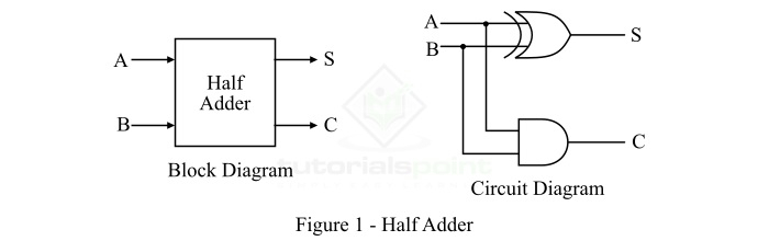
In the half adder, the output of the XOR gate is the sum of two bits and the output of the AND gate is the carry bit. However, in the half-adder circuit, the carry obtained in one addition will not be forwarded in the next addition.
The output equation of the half adder are,
$$\mathrm{Sum, \: S \: = \: A \: \oplus \: B}$$
$$\mathrm{Carry, \: C \: = \: A \: \cdot \ B}$$
What is a Full Adder?
Full adder is also a combinational logic circuit that can add two binary digits (bits) and a carry bit, and produces a sum bit and a carry bit as output.
In other words, a combinational circuit which is designed to add three binary digits and produces two outputs (sum and carry) is known as a full adder. Thus, a full adder circuit adds three binary digits, where two are the inputs and one is the carry forwarded from the previous addition. The block diagram and circuit diagram of the full adder are shown in Figure-2.
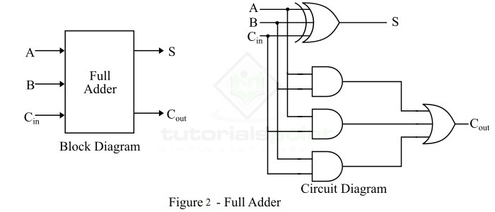
It is clear that the logic circuit of a full adder consists of one XOR gate, three AND gates and one OR gate, which are connected together as shown in Figure-2. Here, A and B are the input bits, Cin is the carry from previous addition, S is the sum bit, and Cout is the output carry bit.
The output equations of the full adder are,
$$\mathrm{Sum, \: S \: = \: A \: \oplus \: B \: \oplus \: C_{in}}$$
$$\mathrm{Carry, \: C_{out} \: = \: Ab \: + \: AC_{in} \: + \: BC_{in}}$$
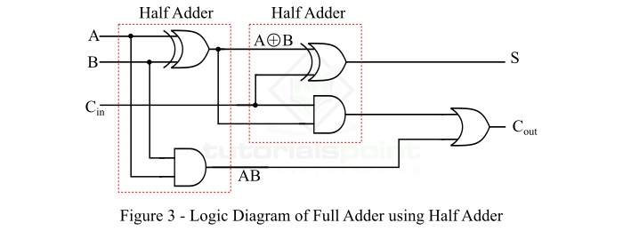
Now, let us discuss the realization of the full adder using half adders
Implementation of Full Adder using Half Adder
The logic diagram of the full adder using two half adders is shown in Figure-3 −
The block diagram of a full adder using two half adders is shown in Figure-4.
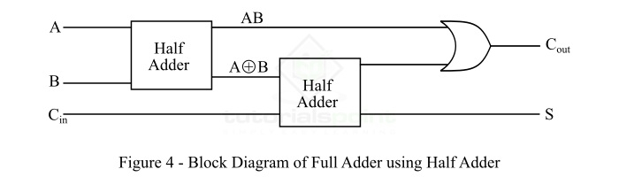
From the logic diagram of the full adder using half adders, it is clear that we require two XOR gates, two AND gates and one OR gate for the implementation of a full adder circuit using half-adders.
However, the implementation of full adder using half adder has a major disadvantage that is the increased propagation delay. That means, the input bits must propagate through several gates in succession that increases the total propagation delay of the full adder circuit.