
- Semiconductor Devices - Home
- Introduction
- Atomic Combinations
- Conduction in Solid Materials
- Conductivity & Mobility
- Types of Semiconductor
- Doping in Semiconductors
- Junction Diodes
- Depletion Zone
- Barrier Potential
- Junction Biasing
- Leakage Current
- Diode Characteristics
- Light Emitting Diode
- Zener Diode
- Photo Diode
- Photovoltaic Cells
- Varactor Diode
- Bipolar Transistors
- Construction of a Transistor
- Transistor Biasing
- Configuration of Transistors
- Field Effect Transistors
- JFET Biasing
- Semiconductor Devices - MOSFET
- Operational Amplifiers
- Practical Op-Amps
- Semiconductor Devices - Integrator
- Differentiator
- Oscillators
- Feedback & Compensation
- Semiconductor Devices - Quick Guide
- Semiconductor Devices - Resources
- Semiconductor Devices - Discussion
Semiconductor Devices - Transistor Biasing
Transistors have three sections namely the emitter, the base, and the collector.
The base is much thinner than the emitter, and the collector is comparatively wider than both.
The emitter is heavily doped so that it can inject large number of charge carriers for current conduction.
The base passes most of the charge carriers to the collector as it is comparatively lightly doped than emitter and the collector.
For a proper functioning of the transistor, the emitter-base region must be forward-biased and collector-base region must be reverse-biased.
In semiconductor circuits, the source voltage is called as the bias voltage. In order to function, bipolar transistors must have both junctions biased. This condition causes a current to flow through the circuit. The depletion region of the device is reduced and majority current carriers are injected towards the junction. One of the junctions of a transistor must be forward biased and other must be reverse biased when it operates.
Working of NPN Transistor
As shown in the above figure, the emitter to base junction is forward biased and the collector to base junction is reverse biased. Forward bias on the emitter to base junction causes the electrons to flow from N type emitter towards the bias. This condition formulates the emitter current (IE).
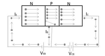
While crossing the P-type material, electrons tend to combine with holes, generally very few, and constitute the base current (IB). Rest of the electrons cross the thin depletion region and reach the collector region. This current constitutes collector current (IC).
In other words, the emitter current actually flows through the collector circuit. Therefore, it can be considered that the emitter current is the summation of the base and the collector current. It can be expressed as,
IE = IB + IC
Working of PNP Transistor
As shown in the following figure, the emitter to base junction is forward biased and the collector to base junction is reverse biased. Forward bias on the emitter to base junction causes the holes to flow from P type emitter towards the bias. This condition formulates the emitter current (IE).
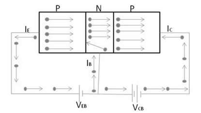
While crossing the N-type material, the electrons tend to combine with electrons, generally very few, and constitute the base current (IB). Rest of the holes cross the thin depletion region and reach the collector region. This current constitutes the collector current (IC).
In other words, the emitter current actually flows through the collector circuit. Therefore, it can be considered that the emitter current is the summation of the base and the collector current. It can be expressed as,
IE = IB + IC