
- Semiconductor Devices - Home
- Introduction
- Atomic Combinations
- Conduction in Solid Materials
- Conductivity & Mobility
- Types of Semiconductor
- Doping in Semiconductors
- Junction Diodes
- Depletion Zone
- Barrier Potential
- Junction Biasing
- Leakage Current
- Diode Characteristics
- Light Emitting Diode
- Zener Diode
- Photo Diode
- Photovoltaic Cells
- Varactor Diode
- Bipolar Transistors
- Construction of a Transistor
- Transistor Biasing
- Configuration of Transistors
- Field Effect Transistors
- JFET Biasing
- Semiconductor Devices - MOSFET
- Operational Amplifiers
- Practical Op-Amps
- Semiconductor Devices - Integrator
- Differentiator
- Oscillators
- Feedback & Compensation
- Semiconductor Devices - Quick Guide
- Semiconductor Devices - Resources
- Semiconductor Devices - Discussion
Semiconductor Devices - Depletion Zone
Initially, when a junction diode is formed, there is a unique interaction between current carriers. In N type material, the electrons move readily across the junction to fill holes in the P material. This act is commonly called diffusion. Diffusion is the result of high accumulation of carriers in one material and a lower gathering in the other.
Generally, the current carriers which are near to the junction only takes part in the process of diffusion. Electrons departing the N material cause positive ions to be generated in their place. While entering the P material to fill holes, negative ions are created by these electrons. As a result, each side of the junction contains a large number of positive and negative ions.
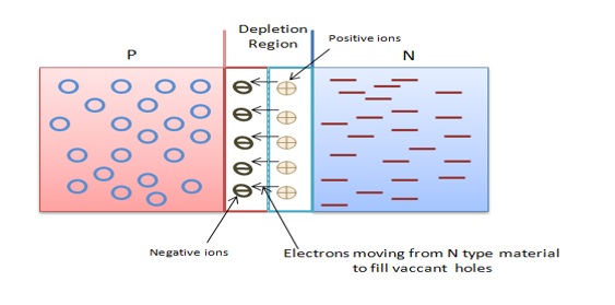
The area where these holes and electrons become depleted is generally known by the term depletion region. It is an area where there is lack of majority current carriers. Normally, a depletion region is developed when P-N junction is formed. The following figure shows the depletion region of a junction diode.