
- Semiconductor Devices - Home
- Introduction
- Atomic Combinations
- Conduction in Solid Materials
- Conductivity & Mobility
- Types of Semiconductor
- Doping in Semiconductors
- Junction Diodes
- Depletion Zone
- Barrier Potential
- Junction Biasing
- Leakage Current
- Diode Characteristics
- Light Emitting Diode
- Zener Diode
- Photo Diode
- Photovoltaic Cells
- Varactor Diode
- Bipolar Transistors
- Construction of a Transistor
- Transistor Biasing
- Configuration of Transistors
- Field Effect Transistors
- JFET Biasing
- Semiconductor Devices - MOSFET
- Operational Amplifiers
- Practical Op-Amps
- Semiconductor Devices - Integrator
- Differentiator
- Oscillators
- Feedback & Compensation
- Semiconductor Devices - Quick Guide
- Semiconductor Devices - Resources
- Semiconductor Devices - Discussion
Doping in Semiconductors
Pure Silicon or Germanium are rarely used as semiconductors. Practically usable semiconductors must have controlled quantity of impurities added to them. Addition of impurity will change the conductor ability and it acts as a semiconductor. The process of adding an impurity to an intrinsic or pure material is called doping and the impurity is called a dopant. After doping, an intrinsic material becomes an extrinsic material. Practically only after doping these materials become usable.
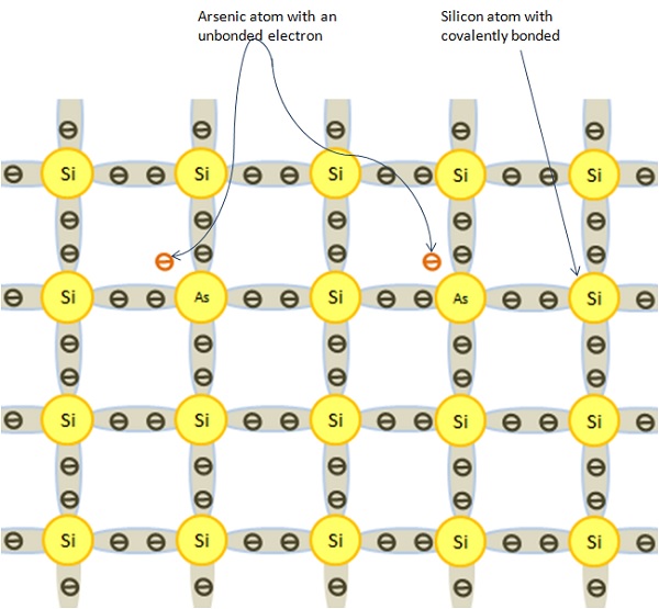
When an impurity is added to silicon or germanium without modifying the crystal structure, an N-type material is produced. In some atoms, electrons have five electrons in their valence band such as arsenic (As) and antimony (Sb). Doping of silicon with either impurity must not change the crystal structure or the bonding process. The extra electron of impurity atom does not take part in a covalent bonding. These electrons are loosely held together by their originator atoms. The following figure shows alteration of silicon crystal with the addition of an impurity atom.
Effect of Doping on N-type Material
The effect of doping on an N-type material is as follows −
On addition of Arsenic to pure Silicon, the crystal becomes an N-type material.
Arsenic atom has additional electrons or negative charges that do not take part in the process of covalent bonding.
These impurities give up or donate, one electron to the crystal and they are referred to as donor impurities.
An N-type material has extra or free electrons than an intrinsic material.
An N-type material is not negatively charged. Actually all of its atoms are all electrically neutral.
These extra electrons do not take part in the covalent bonding process. They are free to move about through the crystal structure.
An N-type extrinsic silicon crystal will go into conduction with only 0.005eV of energy applied.
Only 0.7eV is required to move electrons of intrinsic crystal from the valence band into the conduction band.
Normally, electrons are considered to be the majority current carriers in this type of crystal and holes are the minority current carriers. The quantity of donor material added to Silicon finds out the number of majority current carriers in its structure.
The number of electrons in an N-type silicon is many times greater than the electron-hole pairs of intrinsic silicon. At room temperature, there is a firm difference in the electrical conductivity of this material. There are abundant current carriers to take part in the current flow. The flow of current is achieved mostly by electrons in this type of material. Therefore, an extrinsic material becomes a good electrical conductor.
Effect of Doping on P-type Material
The effect of doping on a P-type material is as follows −
When Indium (In) or Gallium (Ga) is added to pure silicon, a P-type material is formed.
This type of dopant material has three valence electrons. They are eagerly looking for a fourth electron.
In P type material, each hole can be filled with an electron. To fill this hole area, very less energy is required by electrons from the neighboring covalent bonded groups.
Silicon is typically doped with doping material in the range of 1 to 106. This means that P material will have much more holes than the electron-hole pairs of pure silicon.
At room temperature, there is a very determined characteristic difference in the electrical conductivity of this material.
The following figure shows how the crystal structure of Silicon is altered when doped with an acceptor element in this case, Indium. A piece of P material is not positively charged. Its atoms are primarily all electrically neutral.
There are, however, holes in the covalent structure of many atom groups. When an electron moves in and fills a hole, the hole becomes void. A new hole is created in the bonded group where the electron left. Hole movement in effect is the result of electron movement. A P-type material will go into conduction with only 0.05 eV of energy applied.
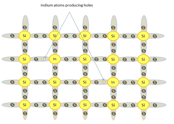
The above figure shows how a P-type crystal will respond when connected to a voltage source. Note that there are larger numbers of holes than electrons. With voltage applied, the electrons are attracted to the positive battery terminal.
Holes move, in a sense, toward the negative battery terminal. An electron is picked up at this point. The electron immediately fills a hole. The hole then becomes void. At the same time, an electron is pulled from the material by the positive battery terminal. Holes therefore move toward the negative terminal due to electrons shifting between different bonded groups. With energy applied, hole flow is continuous.