- Linear Wave Shapping
- Special Functions of LPF and HPF
- Nonlinear Wave Shapping
- Positive Clipper Circuits
- Negative Clipper Circuits
- Clamper Circuits
- Limiter & Voltage Multiplier
- Diode as a Switch
- Power Supplies
- Power Supplies
- Electronic Circuits - Rectifiers
- Full Wave Rectifiers
- Electronic Circuits - Filters
- Electronic Circuits - Regulators
- Electronic Circuits - SMPS
- Electronic Circuits Resources
- Electronic Circuits - Quick Guide
- Electronic Circuits - Resources
- Electronic Circuits - Discussion
Electronic Circuits - Quick Guide
Electronic Circuits - Introduction
In Electronics, we have different components that serve different purposes. There are various elements which are used in many types of circuits depending on the applications.
Electronic Components
Similar to a brick that constructs a wall, a component is the basic brick of a circuit. A Component is a basic element that contributes for the development of an idea into a circuit for execution.
Each component has a few basic properties and the component behaves accordingly. It depends on the motto of the developer to use them for the construction of the intended circuit. The following image shows a few examples of electronic components that are used in different electronic circuits.
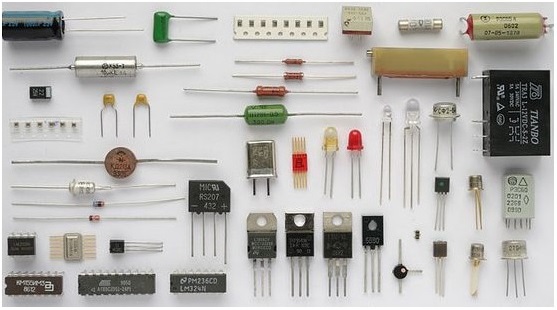
Just to gather an idea, let us look at the types of Components. They can either be Active Components or Passive Components.
Active Components
Active Components are those which conduct upon providing some external energy.
Active Components produce energy in the form of voltage or current.
Examples − Diodes, Transistors, Transformers, etc.
Passive Components
Passive components are those which start their operation once they are connected. No external energy is needed for their operation.
Passive components store and maintain energy in the form of voltage or current.
Examples − Resistors, Capacitors, Inductors, etc.
We also have another classification as Linear and Non-Linear elements.
Linear Components
Linear elements or components are the ones that have linear relationship between current and voltage.
The parameters of linear elements are not changed with respect to current and voltage.
Examples − Diodes, Transistors, Transformers, etc.
Non-linear Components
Non-linear elements or components are the ones that have a non-linear relationship between current and voltage.
The parameters of non-linear elements are changed with respect to current and voltage.
Examples − Resistors, Capacitors, Inductors, etc.
These are the components intended for various purposes, which altogether can perform a preferred task for which they are built. Such a combination of different components is known as a Circuit.
Electronic Circuits
A certain number of components when connected on a purpose in a specific fashion makes a circuit. A circuit is a network of different components. There are different types of circuits.
The following image shows different types of electronic circuits. It shows Printed Circuit Boards which are a group of electronic circuits connected on a board.
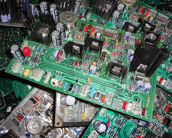
Electronic circuits can be grouped under different categories depending upon their operation, connection, structure, etc. Lets discuss more about the types of Electronic Circuits.
Active Circuit
A circuit that is build using Active components is called as Active Circuit.
It usually contains a power source from which the circuit extracts more power and delivers it to the load.
Additional Power is added to the output and hence output power is always greater than the input power applied.
The power gain will always be greater than unity.
Passive Circuit
A circuit that is build using Passive components is called as Passive Circuit.
Even if it contains a power source, the circuit does not extract any power.
Additional Power is not added to the output and hence output power is always less than the input power applied.
The power gain will always be less than unity.
Electronic circuits can also be classified as Analog, Digital, or Mixed.
Analog Circuit
An analog circuit can be one which has linear components in it. Hence it is a linear circuit.
An analog circuit has analog signal inputs which are continuous range of voltages.
Digital Circuit
A digital circuit can be one which has non-linear components in it. Hence it is a non-linear circuit.
It can process digital signals only.
A digital circuit has digital signal inputs which are discrete values.
Mixed Signal Circuit
A mixed signal circuit can be one which has both linear and non-linear components in it. Hence it is called as a mixed signal circuit.
These circuits consist of analog circuitry along with microprocessors to process the input.
Depending upon the type of connection, circuits can be classified as either Series Circuit or Parallel Circuit. A Series Circuit is one which is connected in series and a parallel circuit is one which has its components connected in parallel.
Now that we have a basic idea about electronic components, let us move on and discuss their purpose which will help us build better circuits for different applications. Whatever might be the purpose of an electronic circuit (to process, to send, to receive, to analyze), the process is carried out in the form of signals. In the next chapter, we will discuss the signals and the type of signals present in electronic circuits.
Electronic Circuits - Signals
A Signal can be understood as "a representation that gives some information about the data present at the source from which it is produced." This is usually time varying. Hence, a signal can be a source of energy which transmits some information. This can easily be represented on a graph.
Examples
- An alarm gives a signal that its time.
- A cooker whistle confirms that the food is cooked.
- A red light signals some danger.
- A traffic signal indicates your move.
- A phone rings signaling a call for you.
A signal can be of any type that conveys some information. This signal produced from an electronic equipment, is called as Electronic Signal or Electrical Signal. These are generally time variants.
Types of Signals
Signals can be classified either as Analog or Digital, depending upon their characteristics. Analog and Digital signals can be further classified, as shown in the following image.
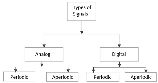
Analog Signal
A continuous time-varying signal, which represents a time-varying quantity, can be termed as an Analog Signal. This signal keeps on varying with respect to time, according to the instantaneous values of the quantity, which represents it.
Digital Signal
A signal which is discrete in nature or which is non-continuous in form can be termed as a Digital signal. This signal has individual values, denoted separately, which are not based on previous values, as if they are derived at that particular instant of time.
Periodic Signal & Aperiodic Signal
Any analog or digital signal, that repeats its pattern over a period of time, is called as a Periodic Signal. This signal has its pattern continued repeatedly and is easy to be assumed or to be calculated.
Any analog or digital signal, that doesnt repeat its pattern over a period of time, is called as Aperiodic Signal. This signal has its pattern continued but the pattern is not repeated and is not so easy to be assumed or to be calculated.
Signals & Notations
Among the Periodic Signals, the most commonly used signals are Sine wave, Cosine wave, Triangular waveform, Square wave, Rectangular wave, Saw-tooth waveform, Pulse waveform or pulse train etc. let us have a look at those waveforms.
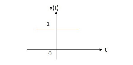
Unit Step Signal
The unit step signal has the value of one unit from its origin to one unit on the X-axis. This is mostly used as a test signal. The image of unit step signal is shown below.
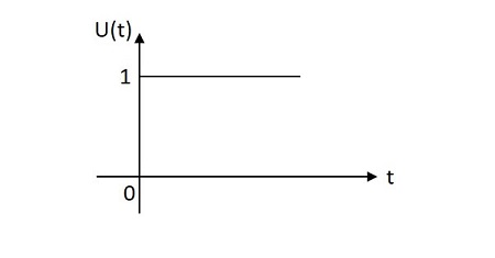
The unit step function is denoted by $u\left ( t \right )$. It is defined as −
$$u\left ( t \right )=\left\{\begin{matrix}1 & t\geq 0\\ 0 & t
Unit Impulse Signal
The unit impulse signal has the value of one unit at its origin. Its area is one unit. The image of unit impulse signal is shown below.
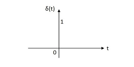
The unit impulse function is denoted by (t). It is defined as
$$\delta \left ( t \right )=\left\{\begin{matrix} \infty \:\:if \:\:t=0\\0 \:\:if \:\:t\neq 0\end{matrix}\right.$$
$$\int_{-\infty }^{\infty }\delta \left ( t \right )d\left ( t \right )=1$$
$$\int_{-\infty }^{t }\delta \left ( t \right )d\left ( t \right )=u\left ( t \right )$$
$$\delta \left ( t \right )=\frac{du\left ( t \right )}{d\left ( t \right )} $$
Unit Ramp Signal
The unit ramp signal has its value increasing exponentially from its origin. The image of unit ramp signal is shown below.
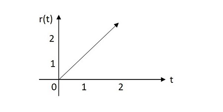
The unit ramp function is denoted by u(t). It is defined as −
$$\int_{0}^{t}u\left ( t \right ) d\left ( t \right )=\int_{0}^{t} 1 dt =t=r\left ( t \right )$$
$$u\left ( t \right )=\frac{dr\left ( t \right )}{dt}$$
Unit Parabolic Signal
The unit parabolic signal has its value altering like a parabola at its origin. The image of unit parabolic signal is shown below.
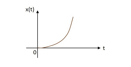
The unit parabolic function is denoted by $u\left ( t \right )$. It is defined as −
$$\int_{0}^{t}\int_{0}^{t}u\left ( t \right )dtdt=\int_{0}^{t}r\left ( t \right )dt=\int_{0}^{t} t.dt=\frac{t^{2}}{2}dt=x\left ( t \right )$$
$$r\left ( t \right )=\frac{dx\left ( t \right )}{dt}$$
$$u\left ( t \right )=\frac{d^{2}x\left ( t \right )}{dt^{2}}$$
Signum Function
The Signum function has its value equally distributed in both positive and negative planes from its origin. The image of Signum function is shown below.
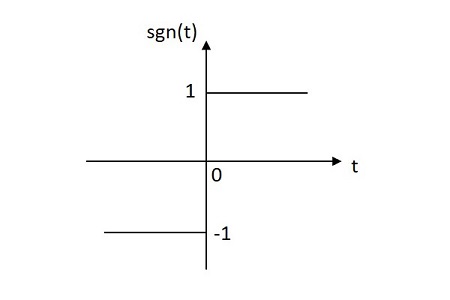
The Signum function is denoted by sgn(t). It is defined as
$$sgn\left ( t \right )=\left\{\begin{matrix} 1 \:\: for \:\: t\geq 0\\-1 \:\: for \:\:t
$$sgn\left ( t \right )=2u\left ( t \right ) -1$$
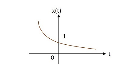
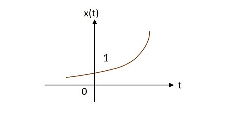
Exponential Signal
The exponential signal has its value varying exponentially from its origin. The exponential function is in the form of −
$$x\left ( t \right ) =e^{\alpha t}$$
The shape of exponential can be defined by $\alpha$. This function can be understood in 3 cases
Case 1 −
If $\alpha = 0\rightarrow x\left ( t \right )=e^{0}=1$
Case 2 −
If $\alpha decaying exponential.
Case 3 −
If $\alpha > 0$ then $x\left ( t \right )=e^{\alpha t}$ where $\alpha$ is positive. This shape is called as raising exponential.
Rectangular Signal
The rectangular signal has its value distributed in rectangular shape in both positive and negative planes from its origin. The image of rectangular signal is shown below.
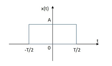
The rectangular function is denoted by $x\left ( t \right )$. It is defined as
$$x\left ( t \right )=A \:rect\left [ \frac{t}{T} \right ]$$
Triangular Signal
The rectangular signal has its value distributed in triangular shape in both positive and negative planes from its origin. The image of triangular signal is shown below.
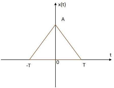
The triangular function is denoted by$x\left ( t \right )$. It is defined as
$$x\left ( t \right )=A \left [ 1-\frac{\left | t \right |}{T} \right ]$$
Sinusoidal Signal
The Sinusoidal signal has its value varying sinusoidally from its origin. The image of Sinusoidal signal is shown below.
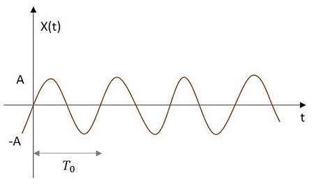
The sinusoidal function is denoted by x (t). It is defined as −
$$x\left ( t \right )=A \cos \left ( w_{0} t\pm \phi \right )$$
or
$$x\left ( t \right )=A sin\left ( w_{0}t\pm \phi \right )$$
Where $T_{0}=\frac{2 \pi}{w_{0}}$
Sinc Function
The Sinc signal has its value varying according to a particular relation as in given equation below. It has its maximum value at the origin and goes on decreasing as it moves away. The image of a Sinc function signal is shown below.
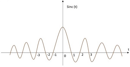
The Sinc function is denoted by sinc(t). It is defined as −
$$sinc\left ( t \right )=\frac{sin\left ( \pi t \right )}{\pi t}$$
So, these are the different signals we mostly come across in the field of Electronics and Communications. Every signal can be defined in a mathematical equation to make the signal analysis easier.
Each signal has a particular wave shape as mentioned before. The shaping of the wave may alter the content present in the signal. Anyways, it is the decision to be made by the design engineer whether to alter a wave or not for any particular circuit. But, to alter the shape of the wave, there are few techniques which will be discussed in further units
Electronic Circuits - Linear Wave Shapping
A Signal can also be called as a Wave. Every wave has a certain shape when it is represented in a graph. This shape can be of different types such as sinusoidal, square, triangular, etc. which vary with respect to time period or they may have some random shapes disregard of the time period.
Types of Wave Shaping
There are two main types of wave shaping. They are −
- Linear wave shaping
- Non-linear wave shaping
Linear Wave Shaping
Linear elements such as resistors, capacitors and inductors are employed to shape a signal in this linear wave shaping. A Sine wave input has a sine wave output and hence the nonsinusoidal inputs are more prominently used to understand the linear wave shaping.
Filtering is the process of attenuating the unwanted signal or to reproduce the selected portions of the frequency components of a particular signal.
Filters
In the process of shaping a signal, if some portions of the signal are felt unwanted, they can be cut off using a Filter Circuit. A Filter is a circuit that can remove unwanted portions of a signal at its input. The process of reduction in the strength of the signal is also termed as Attenuation.
We have few components which help us in filtering techniques.
A Capacitor has the property to allow AC and to block DC
An Inductor has the property to allow DC but blocks AC.
Using these properties, these two components are especially used to block or allow AC or DC. The Filters can be designed depending upon these properties.
We have four main types of filters −
- Low pass filter
- High pass filter
- Band pass filter
- Band stop filter
Let us now discuss these types of filters in detail.
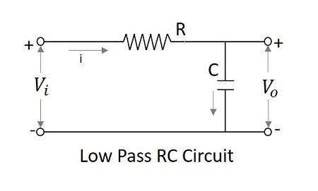
Low Pass Filter
A Filter circuit which allows a set of frequencies that are below a specified value can be termed as a Low pass filter. This filter passes the lower frequencies. The circuit diagram of a low pass filter using RC and RL are as shown below.
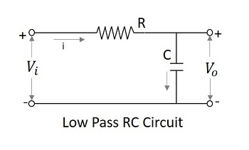
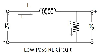
The capacitor filter or RC filter and the inductor filter or RL filter both act as low pass filters.
The RC filter − As the capacitor is placed in shunt, the AC it allows is grounded. This by passes all the high frequency components while allows DC at the output.
The RL filter − As the inductor is placed in series, the DC is allowed to the output. The inductor blocks AC which is not allowed at the output.
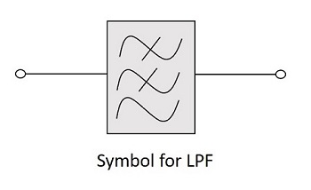
The symbol for a low pass filter (LPF) is as given below.
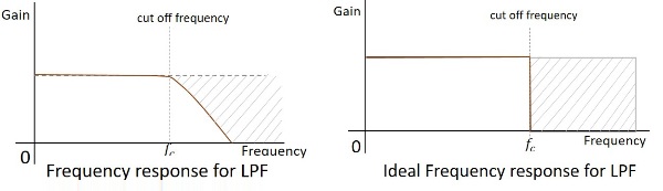
Frequency Response
The frequency response of a practical filter is as shown here under and the frequency response of an ideal LPF when the practical considerations of electronic components are not considered will be as follows.
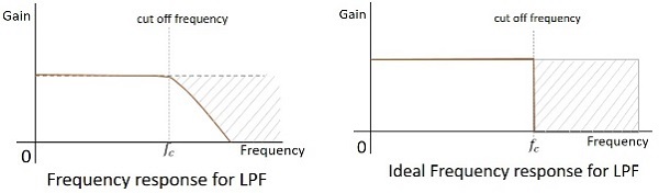
The cut off frequency for any filter is the critical frequency $f_{c}$ for which the filter is intended to attenuate (cut) the signal. An ideal filter has a perfect cut-off whereas a practical one has few limitations.
The RLC Filter
After knowing about the RC and RL filters, one may have an idea that it would be good to add these two circuits in order to have a better response. The following figure shows how the RLC circuit looks like.
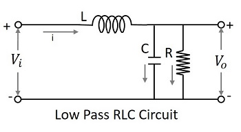
The signal at the input goes through the inductor which blocks AC and allows DC. Now, that output is again passed through the capacitor in shunt, which grounds the remaining AC component if any, present in the signal, allowing DC at the output. Thus we have a pure DC at the output. This is a better low pass circuit than both of them.
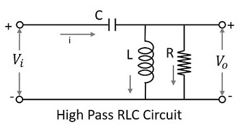
High Pass Filter
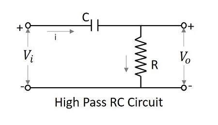
A Filter circuit which allows a set of frequencies that are above a specified value can be termed as a High pass filter. This filter passes the higher frequencies. The circuit diagram of a high pass filter using RC and RL are as shown below.
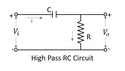
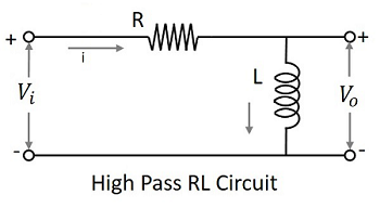
The capacitor filter or RC filter and the inductor filter or RL filter both act as high pass filters.
The RC Filter
As the capacitor is placed in series, it blocks the DC components and allows the AC components to the output. Hence the high frequency components appear at the output across the resistor.
The RL Filter
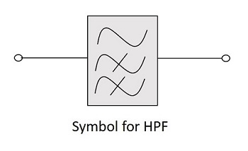
As the inductor is placed in shunt, the DC is allowed to be grounded. The remaining AC component, appears at the output. The symbol for a high pass filter (HPF) is as given below.
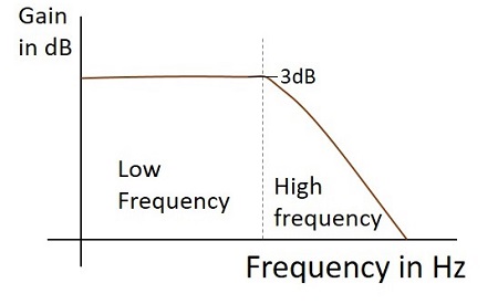
Frequency Response
The frequency response of a practical filter is as shown here under and the frequency response of an ideal HPF when the practical considerations of electronic components are not considered will be as follows.
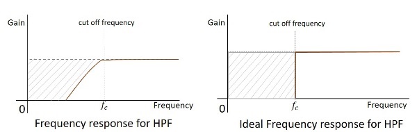
The cut-off frequency for any filter is the critical frequency $f_{c}$ for which the filter is intended to attenuate (cut) the signal. An ideal filter has a perfect cut-off whereas a practical one has few limitations.
The RLC Filter
After knowing about the RC and RL filters, one may have an idea that it would be good to add these two circuits in order to have a better response. The following figure shows how the RLC circuit looks like.
The signal at the input goes through the capacitor which blocks DC and allows AC. Now, that output is again passed through the inductor in shunt, which grounds the remaining DC component if any, present in the signal, allowing AC at the output. Thus we have a pure AC at the output. This is a better high pass circuit than both of them.
Band Pass Filter
A Filter circuit which allows a set of frequencies that are between two specified values can be termed as a Band pass filter. This filter passes a band of frequencies.
As we need to eliminate few of the low and high frequencies, to select a set of specified frequencies, we need to cascade a HPF and a LPF to get a BPF. This can be understood easily even by observing the frequency response curves.
The circuit diagram of a band pass filter is as shown below.
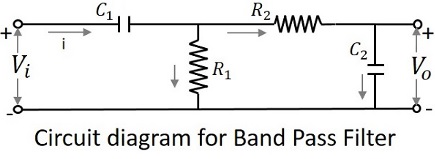
The above circuit can also be constructed using RL circuits or RLC circuits. The above one is a RC circuit chosen for simple understanding.
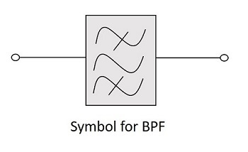
The symbol for a band pass filter (BPF) is as given below.
Frequency Response
The frequency response of a practical filter is as shown here under and the frequency response of an ideal BPF when the practical considerations of electronic components are not considered will be as follows.
The cut-off frequency for any filter is the critical frequency $f_{c}$ for which the filter is intended to attenuate (cut) the signal. An ideal filter has a perfect cut-off whereas a practical one has few limitations.
Band Stop Filter
A Filter circuit which blocks or attenuates a set of frequencies that are between two specified values can be termed as a Band Stop filter. This filter rejects a band of frequencies and hence can also be called as Band Reject Filter.
As we need to eliminate few of the low and high frequencies, to select a set of specified frequencies, we need to cascade a LPF and a HPF to get a BSF. This can be understood easily even by observing the frequency response curves.
The circuit diagram of a band stop filter is as shown below.
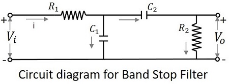
The above circuit can also be constructed using RL circuits or RLC circuits. The above one is a RC circuit chosen for simple understanding.
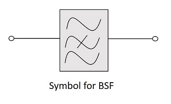
The symbol for a band stop filter (BSF) is as given below.
Frequency Response
The frequency response of a practical filter is as shown here under and the frequency response of an ideal BSF when the practical considerations of electronic components are not considered will be as follows.
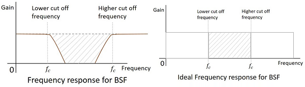
The cut-off frequency for any filter is the critical frequency $f_{c}$ for which the filter is intended to attenuate (cut) the signal. An ideal filter has a perfect cut-off whereas a practical one has few limitations.
Special Functions of LPF and HPF
Low-pass and high-pass filter circuits are used as special circuits in many applications. Low-pass filter (LPF) can work as an Integrator, whereas the high-pass filter (HPF) can work as a Differentiator. These two mathematical functions are possible only with these circuits which reduce the efforts of an electronics engineer in many applications.
Low Pass Filter as Integrator
At low frequencies, the capacitive reactance tends to become infinite and at high frequencies the reactance becomes zero. Hence at low frequencies, the LPF has finite output and at high frequencies the output is nil, which is same for an integrator circuit. Hence low pass filter can be said to be worked as an integrator.
For the LPF to behave as an integrator
$$\tau \gg T$$
Where $\tau = RC$ the time constant of the circuit
Then the voltage variation in C is very small.
$$V_{i}=iR+\frac{1}{C} \int i \:dt$$
$$V_{i}\cong iR$$
$$Since \:\: \frac{1}{C} \int i \:dt \ll iR$$
$$i=\frac{V_{i}}{R}$$
$$ Since \:\: V_{0}=\frac{1}{C}\int i dt =\frac{1}{RC}\int V_{i}dt=\frac{1}{\tau }\int V_{i} dt$$
$$Output \propto \int input$$
Hence a LPF with large time constant produces an output that is proportional to the integral of an input.
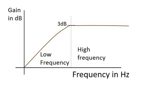
Frequency Response
The Frequency response of a practical low pass filter, when it works as an Integrator is as shown below.
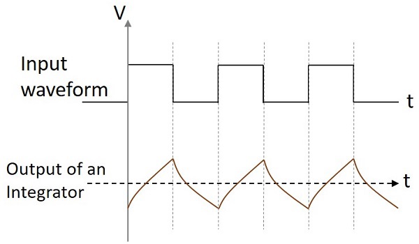
Output Waveform
If the integrator circuit is given a sinewave input, the output will be a cosine wave. If the input is a square wave, the output wave form changes its shape and appears as in the figure below.
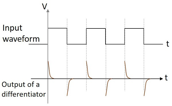
High Pass Filter as Differentiator
At low frequencies, the output of a differentiator is zero whereas at high frequencies, its output is of some finite value. This is same as for a differentiator. Hence the high pass filter is said to be behaved as a differentiator.
If time constant of the RC HPF is very much smaller than time period of the input signal, then circuit behaves as a differentiator. Then the voltage drop across R is very small when compared to the drop across C.
$$V_{i}=\frac{1}{C}\int i \:dt +iR$$
But $iR=V_{0}$ is small
$$since V_{i}=\frac{1}{C}\int i \:dt$$
$$i=\frac{V_{0}}{R}$$
$$Since \: V_{i} =\frac{1}{\tau }\int V_{0} \:dt$$
Where $\tau =RC$ the time constant of the circuit.
Differentiating on both sides,
$$\frac{dV_{i}}{dt}=\frac{V_0}{\tau }$$
$$V_{0}=\tau \frac{dV_{i}}{dt}$$
$$Since \:V_{0}\propto \frac{dV_{i}}{dt}$$
The output is proportional to the differential of the input signal.
Frequency Response
The Frequency response of a practical high pass filter, when it works as a Differentiator is as shown below.
Output Wave form
If the differentiator circuit is given a sinewave input, the output will be a cosine wave. If the input is a square wave, the output wave form changes its shape and appears as in the figure below.
These two circuits are mostly used in various electronic applications. A differentiator circuit produces a constant output voltage when the input applied tends to change steadily. An integrator circuit produces a steadily changing output voltage when the input voltage applied is constant.
Nonlinear Wave Shapping
Along with resistors, the non-linear elements like diodes are used in nonlinear wave shaping circuits to get required altered outputs. Either the shape of the wave is attenuated or the dc level of the wave is altered in the Non-linear wave shaping.
The process of producing non-sinusoidal output wave forms from sinusoidal input, using non-linear elements is called as nonlinear wave shaping.
Clipper Circuits
A Clipper circuit is a circuit that rejects the part of the input wave specified while allowing the remaining portion. The portion of the wave above or below the cut off voltage determined is clipped off or cut off.
The clipping circuits consist of linear and non-linear elements like resistors and diodes but not energy storage elements like capacitors. These clipping circuits have many applications as they are advantageous.
The main advantage of clipping circuits is to eliminate the unwanted noise present in the amplitudes.
These can work as square wave converters, as they can convert sine waves into square waves by clipping.
The amplitude of the desired wave can be maintained at a constant level.
Among the Diode Clippers, the two main types are positive and negative clippers. We will discuss these two types of clippers in the next two chapters.
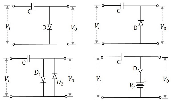
Electronic Circuits - Positive Clipper Circuits
The Clipper circuit that is intended to attenuate positive portions of the input signal can be termed as a Positive Clipper. Among the positive diode clipper circuits, we have the following types −
- Positive Series Clipper
- Positive Series Clipper with positive $V_{r}$ (reference voltage)
- Positive Series Clipper with negative $V_{r}$
- Positive Shunt Clipper
- Positive Shunt Clipper with positive $V_{r}$
- Positive Shunt Clipper with negative $V_{r}$
Let us discuss each of these types in detail.
Positive Series Clipper
A Clipper circuit in which the diode is connected in series to the input signal and that attenuates the positive portions of the waveform, is termed as Positive Series Clipper. The following figure represents the circuit diagram for positive series clipper.
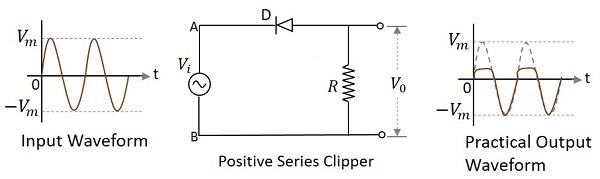
Positive Cycle of the Input − When the input voltage is applied, the positive cycle of the input makes the point A in the circuit positive with respect to the point B. This makes the diode reverse biased and hence it behaves like an open switch. Thus the voltage across the load resistor becomes zero as no current flows through it and hence $V_{0}$ will be zero.
Negative Cycle of the Input − The negative cycle of the input makes the point A in the circuit negative with respect to the point B. This makes the diode forward biased and hence it conducts like a closed switch. Thus the voltage across the load resistor will be equal to the applied input voltage as it completely appears at the output $V_{0}$.
Waveforms
In the above figures, if the waveforms are observed, we can understand that only a portion of the positive peak was clipped. This is because of the voltage across V0. But the ideal output was not meant to be so. Let us have a look at the following figures.
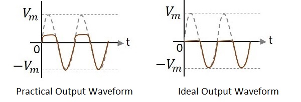
Unlike the ideal output, a bit portion of the positive cycle is present in the practical output due to the diode conduction voltage which is 0.7v. Hence there will be a difference in the practical and ideal output waveforms.
Positive Series Clipper with positive $V_{r}$
A Clipper circuit in which the diode is connected in series to the input signal and biased with positive reference voltage $V_{r}$ and that attenuates the positive portions of the waveform, is termed as Positive Series Clipper with positive $V_{r}$. The following figure represents the circuit diagram for positive series clipper when the reference voltage applied is positive.
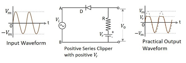
During the positive cycle of the input the diode gets reverse biased and the reference voltage appears at the output. During its negative cycle, the diode gets forward biased and conducts like a closed switch. Hence the output waveform appears as shown in the above figure.
Positive Series Clipper with negative $V_{r}$
A Clipper circuit in which the diode is connected in series to the input signal and biased with negative reference voltage $V_{r}$ and that attenuates the positive portions of the waveform, is termed as Positive Series Clipper with negative $V_{r}$. The following figure represents the circuit diagram for positive series clipper, when the reference voltage applied is negative.
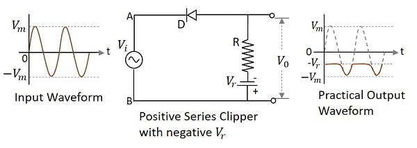
During the positive cycle of the input the diode gets reverse biased and the reference voltage appears at the output. As the reference voltage is negative, the same voltage with constant amplitude is shown. During its negative cycle, the diode gets forward biased and conducts like a closed switch. Hence the input signal that is greater than the reference voltage, appears at the output.
Positive Shunt Clipper
A Clipper circuit in which the diode is connected in shunt to the input signal and that attenuates the positive portions of the waveform, is termed as Positive Shunt Clipper. The following figure represents the circuit diagram for positive shunt clipper.
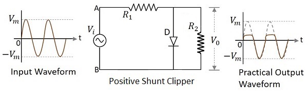
Positive Cycle of the Input − When the input voltage is applied, the positive cycle of the input makes the point A in the circuit positive with respect to the point B. This makes the diode forward biased and hence it conducts like a closed switch. Thus the voltage across the load resistor becomes zero as no current flows through it and hence $V_{0}$ will be zero.
Negative Cycle of the Input − The negative cycle of the input makes the point A in the circuit negative with respect to the point B. This makes the diode reverse biased and hence it behaves like an open switch. Thus the voltage across the load resistor will be equal to the applied input voltage as it completely appears at the output $V_{0}$.
Waveforms
In the above figures, if the waveforms are observed, we can understand that only a portion of the positive peak was clipped. This is because of the voltage across $V_{0}$. But the ideal output was not meant to be so. Let us have a look at the following figures.
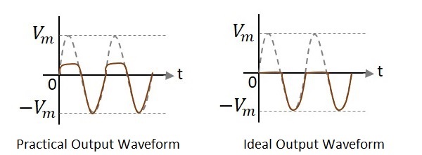
Unlike the ideal output, a bit portion of the positive cycle is present in the practical output due to the diode conduction voltage which is 0.7v. Hence there will be a difference in the practical and ideal output waveforms.
Positive Shunt Clipper with positive $V_{r}$
A Clipper circuit in which the diode is connected in shunt to the input signal and biased with positive reference voltage $V_{r}$ and that attenuates the positive portions of the waveform, is termed as Positive Shunt Clipper with positive $V_{r}$. The following figure represents the circuit diagram for positive shunt clipper when the reference voltage applied is positive.
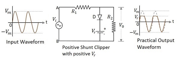
During the positive cycle of the input the diode gets forward biased and nothing but the reference voltage appears at the output. During its negative cycle, the diode gets reverse biased and behaves as an open switch. The whole of the input appears at the output. Hence the output waveform appears as shown in the above figure.
Positive Shunt Clipper with negative $V_{r}$
A Clipper circuit in which the diode is connected in shunt to the input signal and biased with negative reference voltage $V_{r}$ and that attenuates the positive portions of the waveform, is termed as Positive Shunt Clipper with negative $V_{r}$.
The following figure represents the circuit diagram for positive shunt clipper, when the reference voltage applied is negative.
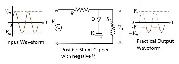
During the positive cycle of the input, the diode gets forward biased and the reference voltage appears at the output. As the reference voltage is negative, the same voltage with constant amplitude is shown. During its negative cycle, the diode gets reverse biased and behaves as an open switch. Hence the input signal that is greater than the reference voltage, appears at the output.
Electronic Circuits - Negative Clipper Circuits
The Clipper circuit that is intended to attenuate negative portions of the input signal can be termed as a Negative Clipper. Among the negative diode clipper circuits, we have the following types.
- Negative Series Clipper
- Negative Series Clipper with positive $V_{r}$ (reference voltage)
- Negative Series Clipper with negative $V_{r}$
- Negative Shunt Clipper
- Negative Shunt Clipper with positive $V_{r}$
- Negative Shunt Clipper with negative $V_{r}$
Let us discuss each of these types in detail.
Negative Series Clipper
A Clipper circuit in which the diode is connected in series to the input signal and that attenuates the negative portions of the waveform, is termed as Negative Series Clipper. The following figure represents the circuit diagram for negative series clipper.
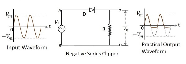
Positive Cycle of the Input − When the input voltage is applied, the positive cycle of the input makes the point A in the circuit positive with respect to the point B. This makes the diode forward biased and hence it acts like a closed switch. Thus the input voltage completely appears across the load resistor to produce the output $V_{0}$.
Negative Cycle of the Input − The negative cycle of the input makes the point A in the circuit negative with respect to the point B. This makes the diode reverse biased and hence it acts like an open switch. Thus the voltage across the load resistor will be zero making $V_{0}$ zero.
Waveforms
In the above figures, if the waveforms are observed, we can understand that only a portion of the negative peak was clipped. This is because of the voltage across $V_{0}$. But the ideal output was not meant to be so. Let us have a look at the following figures.
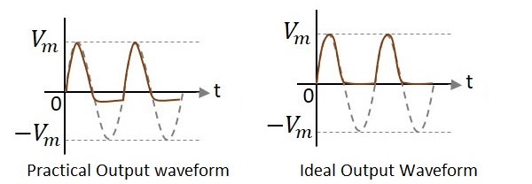
Unlike the ideal output, a bit portion of the negative cycle is present in the practical output due to the diode conduction voltage which is 0.7v. Hence there will be a difference in the practical and ideal output waveforms.
Negative Series Clipper with positive $V_{r}$
A Clipper circuit in which the diode is connected in series to the input signal and biased with positive reference voltage $V_{r}$ and that attenuates the negative portions of the waveform, is termed as Negative Series Clipper with positive $V_{r}$. The following figure represents the circuit diagram for negative series clipper when the reference voltage applied is positive.
During the positive cycle of the input, the diode starts conducting only when the anode voltage value exceeds the cathode voltage value of the diode. As the cathode voltage equals the reference voltage applied, the output will be as shown.
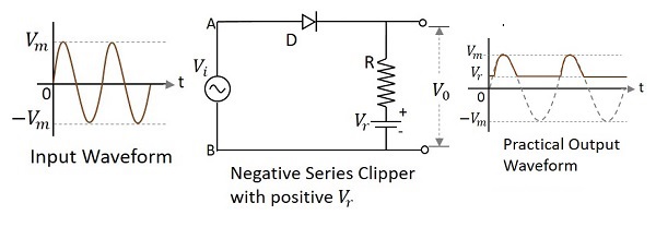
Negative Series Clipper with negative $V_{r}$
A Clipper circuit in which the diode is connected in series to the input signal and biased with negative reference voltage $V_{r}$ and that attenuates the negative portions of the waveform, is termed as Negative Series Clipper with negative $V_{r}$. The following figure represents the circuit diagram for negative series clipper, when the reference voltage applied is negative.
During the positive cycle of the input the diode gets forward biased and the input signal appears at the output. During its negative cycle, the diode gets reverse biased and hence will not conduct. But the negative reference voltage being applied, appears at the output. Hence the negative cycle of the output waveform gets clipped after this reference level.
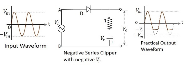
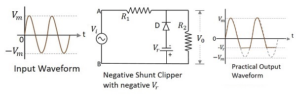
Negative Shunt Clipper
A Clipper circuit in which the diode is connected in shunt to the input signal and that attenuates the negative portions of the waveform, is termed as Negative Shunt Clipper. The following figure represents the circuit diagram for negative shunt clipper.
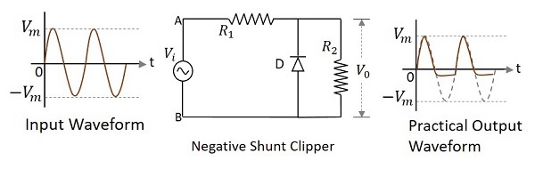
Positive Cycle of the Input − When the input voltage is applied, the positive cycle of the input makes the point A in the circuit positive with respect to the point B. This makes the diode reverse biased and hence it behaves like an open switch. Thus the voltage across the load resistor equals the applied input voltage as it completely appears at the output $V_{0}$
Negative Cycle of the Input − The negative cycle of the input makes the point A in the circuit negative with respect to the point B. This makes the diode forward biased and hence it conducts like a closed switch. Thus the voltage across the load resistor becomes zero as no current flows through it.
Waveforms
In the above figures, if the waveforms are observed, we can understand that just a portion of the negative peak was clipped. This is because of the voltage across $V_{0}$. But the ideal output was not meant to be so. Let us have a look at the following figures.
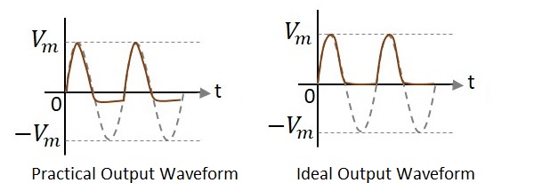
Unlike the ideal output, a bit portion of the negative cycle is present in the practical output due to the diode conduction voltage which is 0.7v. Hence there will be a difference in the practical and ideal output waveforms.
Negative Shunt Clipper with positive $V_{r}$
A Clipper circuit in which the diode is connected in shunt to the input signal and biased with positive reference voltage $V_{r}$ and that attenuates the negative portions of the waveform, is termed as Negative Shunt Clipper with positive $V_{r}$. The following figure represents the circuit diagram for negative shunt clipper when the reference voltage applied is positive.
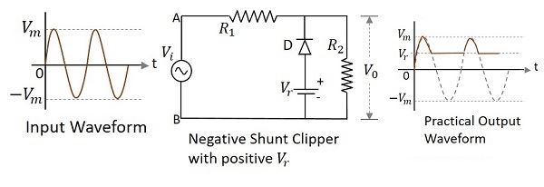
During the positive cycle of the input the diode gets reverse biased and behaves as an open switch. So whole of the input voltage, which is greater than the reference voltage applied, appears at the output. The signal below reference voltage level gets clipped off.
During the negative half cycle, as the diode gets forward biased and the loop gets completed, no output is present.
Negative Shunt Clipper with negative $V_{r}$
A Clipper circuit in which the diode is connected in shunt to the input signal and biased with negative reference voltage $V_{r}$ and that attenuates the negative portions of the waveform, is termed as Negative Shunt Clipper with negative $V_{r}$. The following figure represents the circuit diagram for negative shunt clipper, when the reference voltage applied is negative.
During the positive cycle of the input the diode gets reverse biased and behaves as an open switch. So whole of the input voltage, appears at the output $V_{o}$. During the negative half cycle, the diode gets forward biased. The negative voltage up to the reference voltage, gets at the output and the remaining signal gets clipped off.
Two-way Clipper
This is a positive and negative clipper with a reference voltage $V_{r}$. The input voltage is clipped two-way both positive and negative portions of the input waveform with two reference voltages. For this, two diodes $D_{1}$ and $D_{2}$ along with two reference voltages $V_{r1}$ and $V_{r2}$ are connected in the circuit.
This circuit is also called as a Combinational Clipper circuit. The figure below shows the circuit arrangement for a two-way or a combinational clipper circuit along with its output waveform.
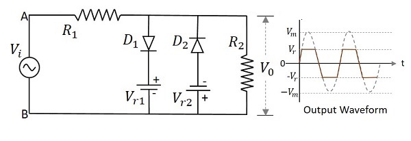
During the positive half of the input signal, the diode $D_{1}$ conducts making the reference voltage $V_{r1}$ appear at the output. During the negative half of the input signal, the diode $D_{2}$ conducts making the reference voltage $V_{r1}$ appear at the output. Hence both the diodes conduct alternatively to clip the output during both the cycles. The output is taken across the load resistor.
With this, we are done with the major clipper circuits. Let us go for the clamper circuits in the next chapter.
Electronic Circuits - Clamper Circuits
A Clamper Circuit is a circuit that adds a DC level to an AC signal. Actually, the positive and negative peaks of the signals can be placed at desired levels using the clamping circuits. As the DC level gets shifted, a clamper circuit is called as a Level Shifter.
Clamper circuits consist of energy storage elements like capacitors. A simple clamper circuit comprises of a capacitor, a diode, a resistor and a dc battery if required.
Clamper Circuit
A Clamper circuit can be defined as the circuit that consists of a diode, a resistor and a capacitor that shifts the waveform to a desired DC level without changing the actual appearance of the applied signal.
In order to maintain the time period of the wave form, the tau must be greater than, half the time period (discharging time of the capacitor should be slow.)
$$\tau = Rc$$
Where
- R is the resistance of the resistor employed
- C is the capacitance of the capacitor used
The time constant of charge and discharge of the capacitor determines the output of a clamper circuit.
In a clamper circuit, a vertical shift of upward or downward takes place in the output waveform with respect to the input signal.
The load resistor and the capacitor affect the waveform. So, the discharging time of the capacitor should be large enough.
The DC component present in the input is rejected when a capacitor coupled network is used (as a capacitor blocks dc). Hence when dc needs to be restored, clamping circuit is used.
Types of Clampers
There are few types of clamper circuits, such as
- Positive Clamper
- Positive clamper with positive $V_r$
- Positive clamper with negative $V_r$
- Negative Clamper
- Negative clamper with positive $V_{r}$
- Negative clamper with negative $V_{r}$
Let us go through them in detail.
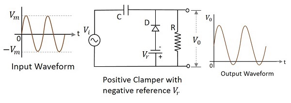
Positive Clamper Circuit
A Clamping circuit restores the DC level. When a negative peak of the signal is raised above to the zero level, then the signal is said to be positively clamped.
A Positive Clamper circuit is one that consists of a diode, a resistor and a capacitor and that shifts the output signal to the positive portion of the input signal. The figure below explains the construction of a positive clamper circuit.
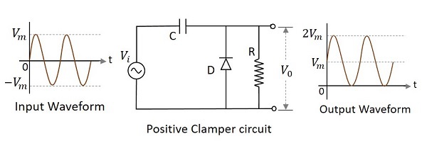
Initially when the input is given, the capacitor is not yet charged and the diode is reverse biased. The output is not considered at this point of time. During the negative half cycle, at the peak value, the capacitor gets charged with negative on one plate and positive on the other. The capacitor is now charged to its peak value $V_{m}$. The diode is forward biased and conducts heavily.
During the next positive half cycle, the capacitor is charged to positive Vm while the diode gets reverse biased and gets open circuited. The output of the circuit at this moment will be
$$V_{0}=V_{i}+V_{m}$$
Hence the signal is positively clamped as shown in the above figure. The output signal changes according to the changes in the input, but shifts the level according to the charge on the capacitor, as it adds the input voltage.
Positive Clamper with Positive Vr
A Positive clamper circuit if biased with some positive reference voltage, that voltage will be added to the output to raise the clamped level. Using this, the circuit of the positive clamper with positive reference voltage is constructed as below.
During the positive half cycle, the reference voltage is applied through the diode at the output and as the input voltage increases, the cathode voltage of the diode increase with respect to the anode voltage and hence it stops conducting. During the negative half cycle, the diode gets forward biased and starts conducting. The voltage across the capacitor and the reference voltage together maintain the output voltage level.
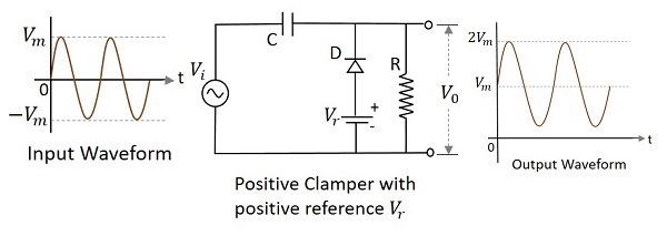
Positive Clamper with Negative $V_{r}$
A Positive clamper circuit if biased with some negative reference voltage, that voltage will be added to the output to raise the clamped level. Using this, the circuit of the positive clamper with positive reference voltage is constructed as below.
During the positive half cycle, the voltage across the capacitor and the reference voltage together maintain the output voltage level. During the negative half-cycle, the diode conducts when the cathode voltage gets less than the anode voltage. These changes make the output voltage as shown in the above figure.
Negative Clamper
A Negative Clamper circuit is one that consists of a diode, a resistor and a capacitor and that shifts the output signal to the negative portion of the input signal. The figure below explains the construction of a negative clamper circuit.
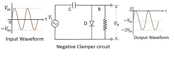
During the positive half cycle, the capacitor gets charged to its peak value $v_{m}$. The diode is forward biased and conducts. During the negative half cycle, the diode gets reverse biased and gets open circuited. The output of the circuit at this moment will be
$$V_{0}=V_{i}+V_{m}$$
Hence the signal is negatively clamped as shown in the above figure. The output signal changes according to the changes in the input, but shifts the level according to the charge on the capacitor, as it adds the input voltage.
Negative clamper with positive Vr
A Negative clamper circuit if biased with some positive reference voltage, that voltage will be added to the output to raise the clamped level. Using this, the circuit of the negative clamper with positive reference voltage is constructed as below.
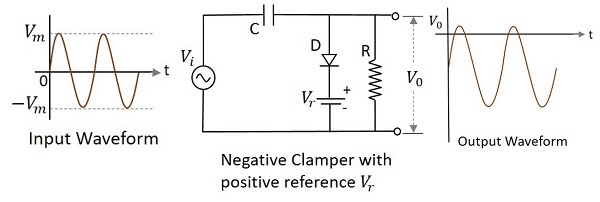
Though the output voltage is negatively clamped, a portion of the output waveform is raised to the positive level, as the applied reference voltage is positive. During the positive half-cycle, the diode conducts, but the output equals the positive reference voltage applied. During the negative half cycle, the diode acts as open circuited and the voltage across the capacitor forms the output.
Negative Clamper with Negative Vr
A Negative clamper circuit if biased with some negative reference voltage, that voltage will be added to the output to raise the clamped level. Using this, the circuit of the negative clamper with negative reference voltage is constructed as below.
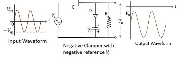
The cathode of the diode is connected with a negative reference voltage, which is less than that of zero and the anode voltage. Hence the diode starts conducting during positive half cycle, before the zero voltage level. During the negative half cycle, the voltage across the capacitor appears at the output. Thus the waveform is clamped towards the negative portion.
Applications
There are many applications for both Clippers and Clampers such as
Clippers
- Used for the generation and shaping of waveforms
- Used for the protection of circuits from spikes
- Used for amplitude restorers
- Used as voltage limiters
- Used in television circuits
- Used in FM transmitters
Clampers
- Used as direct current restorers
- Used to remove distortions
- Used as voltage multipliers
- Used for the protection of amplifiers
- Used as test equipment
- Used as base-line stabilizer
Limiter and Voltage Multiplier
Along with the wave shaping circuits such as clippers and clampers, diodes are used to construct other circuits such as limiters and voltage multipliers, which we shall discuss in this chapter. Diodes also have another important application known as rectifiers, which will be discussed later.
Limiters
Another name which we often come across while going through these clippers and clampers is the limiter circuit. A limiter circuit can be understood as the one which limits the output voltage from exceeding a pre-determined value.
This is more or less a clipper circuit which does not allow the specified value of the signal to exceed. Actually clipping can be termed as an extreme extent of limiting. Hence limiting can be understood as a smooth clipping.
The following image shows some examples of limiter circuits −
The performance of a limiter circuit can be understood from its transfer characteristic curve. An example for such a curve is as follows.
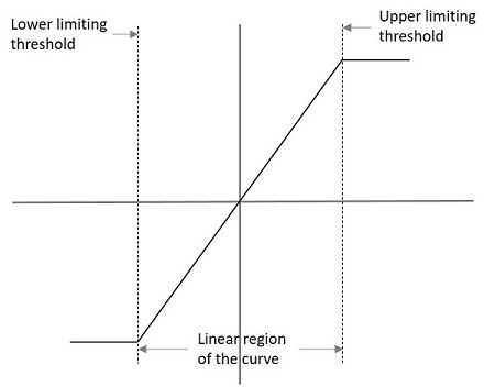
The lower and upper limits are specified in the graph which indicate the limiter characteristics. The output voltage for such a graph can be understood as
$$V_{0}= L_{-},KV_{i},L_{+}$$
Where
$$L_{-}=V_{i}\leq \frac{L_{-}}{k}$$
$$KV_{i}=\frac{L_{-}}{k}
$$L_{+}=V_{i}\geq \frac{L_{+}}{K}$$
Types of Limiters
There are few types of limiters such as
Unipolar Limiter − This circuit limits the signal in one way.
Bipolar Limiter − This circuit limits the signal in two way.
Soft Limiter − The output may change in this circuit for even a slight change in the input.
Hard Limiter − The output will not easily change with the change in input signal.
Single Limiter − This circuit employs one diode for limiting.
Double Limiter − This circuit employs two diodes for limiting.
Voltage Multipliers
There are applications where the voltage needs to be multiplied in some cases. This can be done easily with the help of a simple circuit using diodes and capacitors. The voltage if doubled, such a circuit is called as a Voltage Doubler. This can be extended to make a Voltage Tripler or a Voltage Quadrupler or so on to obtain high DC voltages.
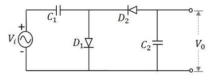
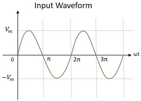
To get a better understanding, let us consider a circuit that multiplies the voltage by a factor of 2. This circuit can be called as a Voltage Doubler. The following figure shows the circuit of a voltage doubler.
The input voltage applied will be an AC signal which is in the form of a sine wave as shown in the figure below.
Working
The voltage multiplier circuit can be understood by analyzing each half cycle of the input signal. Each cycle makes the diodes and the capacitors work in different fashion. Let us try to understand this.
During the first positive half cycle − When the input signal is applied, the capacitor $C_{1}$ is charged and the diode $D_{1}$ is forward biased. While the diode $D_{2}$ is reverse biased and the capacitor $C_{2}$ doesnt get any charge. This makes the output $V_{0}$ to be $V_{m}$
This can be understood from the following figure.
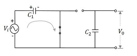
Hence, during 0 to $\pi$, the output voltage produced will be $V_{max}$. The capacitor $C_{1}$ gets charged through the forward biased diode $D_{1}$ to give the output, while $C_{2}$ doesnt charge. This voltage appears at the output.
During the negative half cycle − After that, when the negative half cycle arrives, the diode $D_{1}$ gets reverse biased and the diode $D_{2}$ gets forward biased. The diode $D_{2}$ gets the charge through the capacitor $C_{2}$ which gets charged during this process. The current then flows through the capacitor $C_{1}$ which discharges. It can be understood from the following figure.
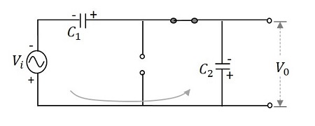
Hence during $\pi$ to $2\pi$, the voltage across the capacitor $C_{2}$ will be $V_{max}$. While the capacitor $C_{1}$ which is fully charged, tends to discharge. Now the voltages from both the capacitors together appear at the output, which is $2V_{max}$. So, the output voltage $V_{0}$ during this cycle is $2V_{max}$
During the next positive half cycle − The capacitor $C_{1}$ gets charged from the supply and the diode $D_{1}$ gets forward biased. The capacitor $C_{2}$ holds the charge as it will not find a way to discharge and the diode $D_{2}$ gets reverse biased. Now, the output voltage $V_{0}$ of this cycle gets the voltages from both the capacitors that together appear at the output, which is $2V_{max}$.
During the next negative half cycle − The next negative half cycle makes the capacitor $C_{1}$ to again discharge from its full charge and the diode $D_{1}$ to reverse bias while $D_{2}$ forward and capacitor $C_{2}$ to charge further to maintain its voltage. Now, the output voltage $V_{0}$ of this cycle gets the voltages from both the capacitors that together appear at the output, which is $2V_{max}$.
Hence, the output voltage $V_{0}$ is maintained to be $2V_{max}$ throughout its operation, which makes the circuit a voltage doubler.
Voltage multipliers are mostly used where high DC voltages are required. For example, cathode ray tubes and computer display.
Voltage Divider
While diodes are used to multiply the voltage, a set of series resistors can be made into a small network to divide the voltage. Such networks are called as Voltage Divider networks.
Voltage divider is a circuit which turns a larger voltage into a smaller one. This is done using resistors connected in series. The output will be a fraction of the input. The output voltage depends upon the resistance of the load it drives.
Let us try to know how a voltage divider circuit works. The figure below is an example of a simple voltage divider network.
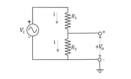
If we try to draw an expression for output voltage,
$$V_{i}=i\left ( R_{1}+R_{2} \right )$$
$$i=\frac{V-{i}}{\left ( R_{1}+R_{2} \right )}$$
$$V_{0}=i \:R_{2}\rightarrow \:i\:=\frac{V_{0}}{R_{2}}$$
Comparing both,
$$\frac{V_{0}}{R_{2}}=\frac{V_{i}}{\left ( R_1 + R_{2} \right )}$$
$$V_{0}=\frac{V_{i}}{\left ( R_1 + R_{2} \right )}R_{2}$$
This is the expression to obtain the value of output voltage. Hence the output voltage is divided depending upon the resistance values of the resistors in the network. More resistors are added to have different fractions of different output voltages.
Let us have an example problem to understand more about voltage dividers.
Example
Calculate the output voltage of a network having an input voltage of 10v with two series resistors 2k and 5k.
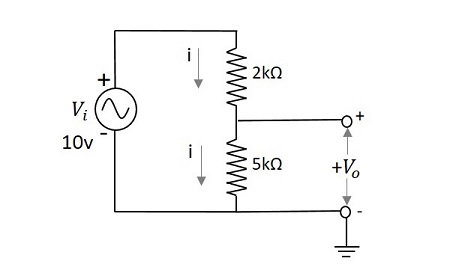
The output voltage $V_{0}$ is given by
$$V_{0}=\frac{V_{i}}{\left ( R_1 + R_{2} \right )}R_{2}$$
$$=\frac{10}{\left ( 2 + 5 \right )k\Omega }5k\Omega$$
$$=\frac{10}{7}\times 5=\frac{50}{7}$$
$$=7.142v$$
The output voltage $V_0$ for the above problem is 7.14v
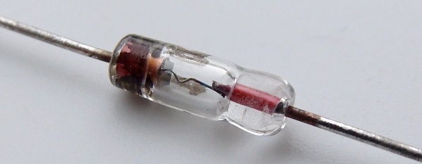
Electronic Circuits - Diode as a Switch
Diode is a two terminal PN junction that can be used in various applications. One of such applications is an electrical switch. The PN junction, when forward biased acts as close circuited and when reverse biased acts as open circuited. Hence the change of forward and reverse biased states makes the diode work as a switch, the forward being ON and the reverse being OFF state.
Electrical Switches over Mechanical Switches
Electrical switches are a preferred choice over mechanical switches due to the following reasons −
- Mechanical switches are prone to oxidation of metals whereas electrical switches dont.
- Mechanical switches have movable contacts.
- They are more prone to stress and strain than electrical switches.
- The worn and torn of mechanical switches often affect their working.
Hence an electrical switch is more useful than a Mechanical switch.
Working of Diode as a Switch
Whenever a specified voltage is exceeded, the diode resistance gets increased, making the diode reverse biased and it acts as an open switch. Whenever the voltage applied is below the reference voltage, the diode resistance gets decreased, making the diode forward biased, and it acts as a closed switch.
The following circuit explains the diode acting as a switch.
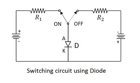
A switching diode has a PN junction in which P-region is lightly doped and N-region is heavily doped. The above circuit symbolizes that the diode gets ON when positive voltage forward biases the diode and it gets OFF when negative voltage reverse biases the diode.
Ringing
As the forward current flows till then, with a sudden reverse voltage, the reverse current flows for an instance rather than getting switched OFF immediately. The higher the leakage current, the greater the loss. The flow of reverse current when diode is reverse biased suddenly, may sometimes create few oscillations, called as RINGING.
This ringing condition is a loss and hence should be minimized. To do this, the switching times of the diode should be understood.
Diode Switching Times
While changing the bias conditions, the diode undergoes a transient response. The response of a system to any sudden change from an equilibrium position is called as transient response.
The sudden change from forward to reverse and from reverse to forward bias, affects the circuit. The time taken to respond to such sudden changes is the important criterion to define the effectiveness of an electrical switch.
The time taken before the diode recovers its steady state is called as Recovery Time.
The time interval taken by the diode to switch from reverse biased state to forward biased state is called as Forward Recovery Time.($t_{fr}$)
The time interval taken by the diode to switch from forward biased state to reverse biased state is called as Reverse Recovery Time. ($t_{fr}$)
To understand this more clearly, let us try to analyze what happens once the voltage is applied to a switching PN diode.
Carrier Concentration
Minority charge carrier concentration reduces exponentially as seen away from the junction. When the voltage is applied, due to the forward biased condition, the majority carriers of one side move towards the other. They become minority carriers of the other side. This concentration will be more at the junction.
For example, if N-type is considered, the excess of holes that enter into N-type after applying forward bias, adds to the already present minority carriers of N-type material.
Let us consider few notations.
- The majority carriers in P-type (holes) = $P_{po}$
- The majority carriers in N-type (electrons) = $N_{no}$
- The minority carriers in P-type (electrons) = $N_{po}$
- The majority carriers in N-type (holes) = $P_{no}$
During Forward biased Condition − The minority carriers are more near junction and less far away from the junction. The graph below explains this.
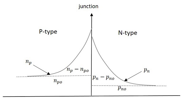
Excess minority carrier charge in P-type = $P_n-P_{no}$ with $p_{no}$ (steady state value)
Excess minority carrier charge in N-type = $N_p-N_{po}$ with $N_{po}$ (steady state value)
During reverse bias condition − Majority carriers doesnt conduct the current through the junction and hence dont participate in current condition. The switching diode behaves as a short circuited for an instance in reverse direction.
The minority carriers will cross the junction and conduct the current, which is called as Reverse Saturation Current. The following graph represents the condition during reverse bias.
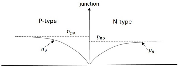
In the above figure, the dotted line represents equilibrium values and solid lines represent actual values. As the current due to minority charge carriers is large enough to conduct, the circuit will be ON until this excess charge is removed.
The time required for the diode to change from forward bias to reverse bias is called Reverse recovery time ($t_{rr}$). The following graphs explain the diode switching times in detail.
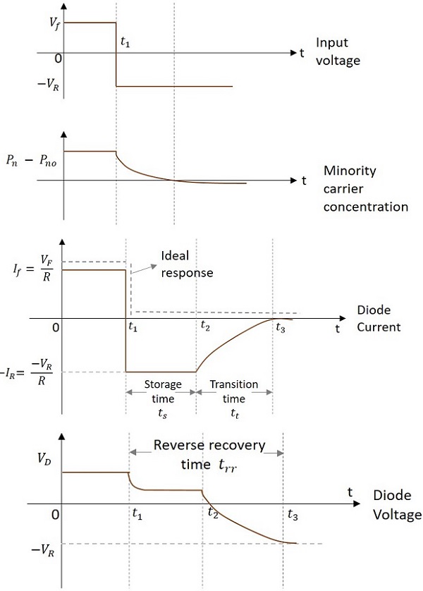
From the above figure, let us consider the diode current graph.
At $t_{1}$ the diode is suddenly brought to OFF state from ON state; it is known as Storage time. Storage time is the time required to remove the excess minority carrier charge. The negative current flowing from N to P type material is of a considerable amount during the Storage time. This negative current is,
$$-I_R= \frac{-V_{R}}{R}$$
The next time period is the transition time (from $t_2$ to $t_3$)
Transition time is the time taken for the diode to get completely to open circuit condition. After $t_3$ diode will be in steady state reverse bias condition. Before $t_1$ diode is under steady state forward bias condition.
So, the time taken to get completely to open circuit condition is
$$Reverse \:\:recovery\:\: time\left ( t_{rr} \right )= Storage \:\:time \left ( T_{s} \right )+Transition \:\: time \left ( T_{t} \right )$$
Whereas to get to ON condition from OFF, it takes less time called as Forward recovery time. Reverse recovery time is greater than Forward recovery time. A diode works as a better switch if this Reverse recovery time is made less.
Definitions
Let us just go through the definitions of the time periods discussed.
Storage time − The time period for which the diode remains in the conduction state even in the reverse biased state, is called as Storage time.
Transition time − The time elapsed in returning back to the state of non-conduction, i.e. steady state reverse bias, is called Transition time.
Reverse recovery time − The time required for the diode to change from forward bias to reverse bias is called as Reverse recovery time.
Forward recovery time − The time required for the diode to change from reverse bias to forward bias is called as Forward recovery time.
Factors that affect diode switching times
There are few factors that affect the diode switching times, such as
Diode Capacitance − The PN junction capacitance changes depending upon the bias conditions.
Diode Resistance − The resistance offered by the diode to change its state.
Doping Concentration − The level of doping of the diode, affects the diode switching times.
Depletion Width − The narrower the width of the depletion layer, the faster the switching will be. A Zener diode has narrow depletion region than an avalanche diode, which makes the former a better switch.
Applications
There are many applications in which diode switching circuits are used, such as −
- High speed rectifying circuits
- High speed switching circuits
- RF receivers
- General purpose applications
- Consumer applications
- Automotive applications
- Telecom applications etc.
Electronic Circuits - Power Supplies
This chapter provides a fresh start regarding another section of diode circuits. This gives an introduction to the Power supply circuits that we come across in our daily life. Any electronic device consists of a power supply unit which provides the required amount of AC or DC power supply to various sections of that electronic device.
Need for Power Supplies
There are many small sections present in the electronic devices such as Computer, Television, Cathode ray Oscilloscope etc. but all of those sections doesnt need 230V AC supply which we get.
Instead one or more sections may need a 12v DC while some others may need a 30v DC. In order to provide the required dc voltages, the incoming 230v AC supply has to be converted into pure DC for the usage. The Power supply units serve the same purpose.
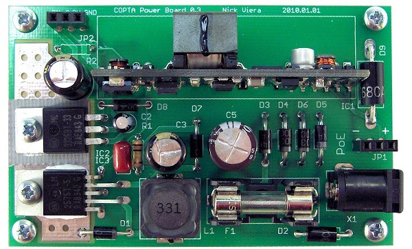
A practical Power supply unit looks as The following figure.
Let us now go through different parts which make a power supply unit.
Parts of a Power supply
A typical Power supply unit consists of the following.
Transformer − An input transformer for the stepping down of the 230v AC power supply.
Rectifier − A Rectifier circuit to convert the AC components present in the signal to DC components.
Smoothing − A filtering circuit to smoothen the variations present in the rectified output.
Regulator − A voltage regulator circuit in order to control the voltage to a desired output level.
Load − The load which uses the pure dc output from the regulated output.
Block Diagram of a Power Supply Unit
The block diagram of a Regulated Power supply unit is as shown below.
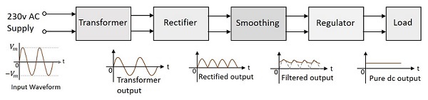
From the diagram above, it is evident that the transformer is present at the initial stage. Though we had already gone through the concept regarding transformers in BASIC ELECTRONICS tutorial, let us have a glance over it.
Transformer
A transformer has a primary coil to which input is given and a secondary coil from which the output is collected. Both of these coils are wound on a core material. Usually an insulator forms the Core of the transformer.
The following figure shows a practical transformer.
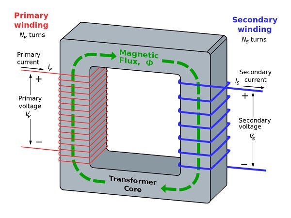
From the above figure, it is evident that a few notations are common. They are as follows −
$N_{p}$ = Number of turns in the primary winding
$N_{s}$ = Number of turns in the secondary winding
$I_{p}$ = Current flowing in the primary of the transformer
$I_{s}$ = Current flowing in the secondary of the transformer
$V_{p}$ = Voltage across the primary of the transformer
$V_{s}$ = Voltage across the secondary of the transformer
$\phi$ = Magnetic flux present around the core of the transformer
Transformer in a Circuit
The following figure shows how a transformer is represented in a circuit. The primary winding, the secondary winding and the core of the transformer are also represented in the following figure.
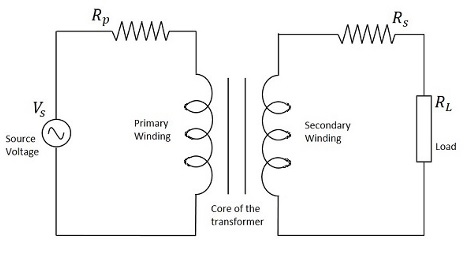
Hence, when a transformer is connected in a circuit, the input supply is given to the primary coil so that it produces varying magnetic flux with this power supply and that flux is induced into the secondary coil of the transformer, which produces the varying EMF of the varying flux. As the flux should be varying, for the transfer of EMF from primary to secondary, a transformer always works on alternating current AC.
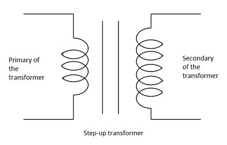
Depending upon the number of turns in the secondary winding, a transformer can be classified either as a Step-up or a Step-down transformer.
Step-Up Transformer
When the secondary winding has more number of turns than the primary winding, then the transformer is said to be a Step-up transformer. Here the induced EMF is greater than the input signal.
The figure below shows the symbol of a step-up transformer.
Step-Down Transformer
When the secondary winding has lesser number of turns than the primary winding, then the transformer is said to be a Step-down transformer. Here the induced EMF is lesser than the input signal.
The figure below shows the symbol of a step-down transformer.
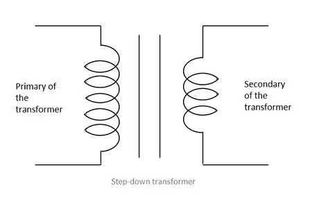
In our Power supply circuits, we use the Step-down transformer, as we need to lessen the AC power to DC. The output of this Step-down transformer will be less in power and this will be given as the input to the next section, called rectifier. We will discuss about rectifiers in the next chapter.
Electronic Circuits - Rectifiers
Whenever there arises the need to convert an AC to DC power, a rectifier circuit comes for the rescue. A simple PN junction diode acts as a rectifier. The forward biasing and reverse biasing conditions of the diode makes the rectification.
Rectification
An alternating current has the property to change its state continuously. This is understood by observing the sine wave by which an alternating current is indicated. It raises in its positive direction goes to a peak positive value, reduces from there to normal and again goes to negative portion and reaches the negative peak and again gets back to normal and goes on.
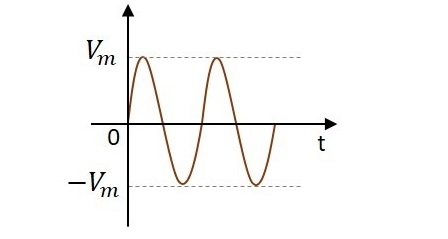
During its journey in the formation of wave, we can observe that the wave goes in positive and negative directions. Actually it alters completely and hence the name alternating current.
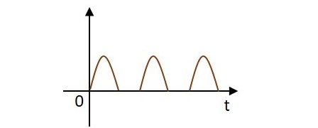
But during the process of rectification, this alternating current is changed into direct current DC. The wave which flows in both positive and negative direction till then, will get its direction restricted only to positive direction, when converted to DC. Hence the current is allowed to flow only in positive direction and resisted in negative direction, just as in the figure below.
The circuit which does rectification is called as a Rectifier circuit. A diode is used as a rectifier, to construct a rectifier circuit.
Types of Rectifier circuits
There are two main types of rectifier circuits, depending upon their output. They are
- Half-wave Rectifier
- Full-wave Rectifier
A Half-wave rectifier circuit rectifies only positive half cycles of the input supply whereas a Full-wave rectifier circuit rectifies both positive and negative half cycles of the input supply.
Half-Wave Rectifier
The name half-wave rectifier itself states that the rectification is done only for half of the cycle. The AC signal is given through an input transformer which steps up or down according to the usage. Mostly a step down transformer is used in rectifier circuits, so as to reduce the input voltage.
The input signal given to the transformer is passed through a PN junction diode which acts as a rectifier. This diode converts the AC voltage into pulsating dc for only the positive half cycles of the input. A load resistor is connected at the end of the circuit. The figure below shows the circuit of a half wave rectifier.
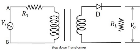
Working of a HWR
TThe input signal is given to the transformer which reduces the voltage levels. The output from the transformer is given to the diode which acts as a rectifier. This diode gets ON (conducts) for positive half cycles of input signal. Hence a current flows in the circuit and there will be a voltage drop across the load resistor. The diode gets OFF (doesnt conduct) for negative half cycles and hence the output for negative half cycles will be, $i_{D} = 0$ and $V_{o}=0$.
Hence the output is present for positive half cycles of the input voltage only (neglecting the reverse leakage current). This output will be pulsating which is taken across the load resistor.
Waveforms of a HWR
The input and output waveforms are as shown in the following figure.
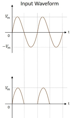
Hence the output of a half wave rectifier is a pulsating dc. Let us try to analyze the above circuit by understanding few values which are obtained from the output of half wave rectifier.
Analysis of Half-Wave Rectifier
To analyze a half-wave rectifier circuit, let us consider the equation of input voltage.
$$v_{i}=V_{m} \sin \omega t$$
$V_{m}$ is the maximum value of supply voltage.
Let us assume that the diode is ideal.
- The resistance in the forward direction, i.e., in the ON state is $R_f$.
- The resistance in the reverse direction, i.e., in the OFF state is $R_r$.
The current i in the diode or the load resistor $R_L$ is given by
$i=I_m \sin \omega t \quad for\quad 0\leq \omega t\leq 2 \pi$
$ i=0 \quad\quad\quad\quad for \quad \pi\leq \omega t\leq 2 \pi$
Where
$$I_m= \frac{V_m}{R_f+R_L}$$
DC Output Current
The average current $I_{dc}$ is given by
$$I_{dc}=\frac{1}{2 \pi}\int_{0}^{2 \pi} i \:d\left ( \omega t \right )$$
$$=\frac{1}{2 \pi}\left [ \int_{0}^{\pi}I_m \sin \omega t \:d\left ( \omega t \right )+\int_{0}^{2 \pi}0\: d\left ( \omega t \right )\right ]$$
$$=\frac{1}{2 \pi}\left [ I_m\left \{-\cos \omega t \right \}_{0}^{\pi} \right ]$$
$$=\frac{1}{2 \pi}\left [ I_m\left \{ +1-\left ( -1 \right ) \right \} \right ]=\frac{I_m}{\pi}=0.318 I_m$$
Substituting the value of $I_m$, we get
$$I_{dc}=\frac{V_m}{\pi\left ( R_f+R_L \right )}$$
If $R_L >> R_f$, then
$$I_{dc}=\frac{V_m}{\pi R_L}=0.318 \frac{V_m}{R_L}$$
DC Output Voltage
The DC output voltage is given by
$$ V_{dc}=I_{dc}\times R_L=\frac{I_m}{\pi}\times R_L$$
$$=\frac{V_m\times R_L}{\pi\left (R_f+R_L \right )}=\frac{V_m}{\pi\left \{ 1+\left ( R_f/R_L \right ) \right \}}$$
If $R_L>>R_f$, then
$$V_{dc}=\frac{V_m}{\pi}=0.318 V_m$$
RMS Current and Voltage
The value of RMS current is given by
$$I_{rms}=\left [ \frac{1}{2 \pi}\int_{0}^{2\pi} i^{2} d\left ( \omega t \right )\right ]^{\frac{1}{2}}$$
$$I_{rms}=\left [ \frac{1}{2 \pi}\int_{0}^{2\pi}I_{m}^{2} \sin^{2}\omega t \:d\left (\omega t \right ) +\frac{1}{2\pi}\int_{\pi}^{2\pi} 0 \:d\left ( \omega t \right )\right ]^{\frac{1}{2}}$$
$$=\left [ \frac{I_{m}^{2}}{2 \pi}\int_{0}^{\pi}\left ( \frac{1-\cos 2 \omega t}{2} \right )d\left ( \omega t \right ) \right ]^{\frac{1}{2}}$$
$$=\left [ \frac{I_{m}^{2}}{4 \pi}\left \{ \left ( \omega t \right )-\frac{\sin 2 \omega t}{2} \right \}_{0}^{\pi}\right ]^{\frac{1}{2}}$$
$$=\left [ \frac{I_{m}^{2}}{4 \pi}\left \{ \pi - 0 - \frac{\sin 2 \pi}{2}+ \sin 0 \right \} \right ]^{\frac{1}{2}}$$
$$=\left [ \frac{I_{m}^{2}}{4 \pi} \right ]^{\frac{1}{2}}=\frac{I_m}{2}$$
$$=\frac{V_m}{2\left ( R_f+R_L \right )}$$
RMS voltage across the load is
$$V_{rms}=I_{rms} \times R_L= \frac{V_m \times R_L}{2\left ( R_f+R_L \right )}$$
$$=\frac{V_m}{2\left \{ 1+\left ( R_f/R_L \right ) \right \}}$$
If $R_L>>R_f$, then
$$V_{rms}=\frac{V_m}{2}$$
Rectifier Efficiency
Any circuit needs to be efficient in its working for a better output. To calculate the efficiency of a half wave rectifier, the ratio of the output power to the input power has to be considered.
The rectifier efficiency is defined as
$$\eta =\frac{d.c.power\:\: delivered \:\: to \:\: the \:\: load}{a.c.input \:\: power\:\:from\:\:transformer\:\:secondary}=\frac{P_{ac}}{P_{dc}}$$
Now
$$P_{dc}=\left ( {I_{dc}} \right )^2 \times R_L=\frac{I_m R_L}{\pi^2}$$
Further
$$P_{ac}=P_a+P_r$$
Where
$P_a = power \:dissipated \:at \:the \:junction \:of \:diode$
$$=I_{rms}^{2}\times R_f=\frac{I_{m}^{2}}{4}\times R_f$$
And
$$P_r = power \:dissipated \:in \:the \:load \:resistance$$
$$=I_{rms}^{2}\times R_L=\frac{I_{m}^{2}}{4}\times R_L$$
$$P_{ac}=\frac{I_{m}^{2}}{4}\times R_f+\frac{I_{m}^{2}}{4}\times R_L =\frac{I_{m}^{2}}{4}\left ( R_f+R_L \right )$$
From both the expressions of $P_{ac}$ and $P_{dc}$, we can write
$$\eta =\frac{I_{m}^{2}R_L/\pi^2}{I_{m}^{2}\left ( R_f+R_L \right )/4}=\frac{4}{\pi^2}\frac{R_L}{\left ( R_f+R_L \right )}$$
$$=\frac{4}{\pi^2}\frac{1}{\left \{ 1+\left ( R_f/R_L \right ) \right \}}=\frac{0.406}{\left \{ 1+\left ( R_f/R_L \right ) \right \}}$$
Percentage rectifier efficiency
$$\eta =\frac{40.6}{\lbrace1+\lgroup\: R_{f}/R_{L}\rgroup\rbrace}$$
Theoretically, the maximum value of rectifier efficiency of a half wave rectifier is 40.6% when $R_{f}/R_{L} = 0$
Further, the efficiency may be calculated in the following way
$$\eta =\frac{P_{dc}}{P_{ac}}=\frac{\left (I_{dc} \right )^2R_L}{\left ( I_{rms} \right )^2R_L}=\frac{\left ( V_{dc}/R_L \right )^2R_L}{\left (V_{rms}/R_L \right )^2R_L} =\frac{\left ( V_{dc} \right )^2}{\left ( V_{rms} \right )^2}$$
$$=\frac{\left ( V_m/ \pi \right )^2}{\left ( V_m/2 \right )^2}=\frac{4}{\pi^2}=0.406$$
$$=40.6\%$$
Ripple Factor
The rectified output contains some amount of AC component present in it, in the form of ripples. This is understood by observing the output waveform of the half wave rectifier. To get a pure dc, we need to have an idea on this component.
The ripple factor gives the waviness of the rectified output. It is denoted by y. This can be defined as the ratio of the effective value of ac component of voltage or current to the direct value or average value.
$$\gamma =\frac{ripple \: voltage}{d.c \:voltage} =\frac{rms\:value\:of\: a.c.component}{d.c.value\:of\:wave}=\frac{\left ( V_r \right )_{rms}}{v_{dc}}$$
Here,
$$\left ( V_r \right )_{rms}=\sqrt{V_{rms}^{2}-V_{dc}^{2}}$$
Therefore,
$$\gamma =\frac{\sqrt{V_{rms}^{2}-V_{dc}^{2}}}{V_{dc}}=\sqrt{\left (\frac{V_{rms}}{V_{dc}} \right )^2-1}$$
Now,
$$V_{rms}=\left [ \frac{1}{2\pi}\int_{0}^{2\pi} V_{m}^{2} \sin^2\omega t\:d\left ( \omega t \right ) \right ]^{\frac{1}{2}}$$
$$=V_m\left [ \frac{1}{4\pi} \int_{0}^{\pi}\left ( 1- \cos2 \:\omega t \right )d\left ( \omega t \right )\right ]^{\frac{1}{2}}=\frac{V_m}{2}$$
$$V_{dc}=V_{av}=\frac{1}{2\pi}\left [ \int_{0}^{\pi}V_m \sin \omega t \:d\left ( \omega t \right )+\int_{0}^{2\pi} 0.d\left ( \omega t \right )\right ]$$
$$=\frac{V_m}{2 \pi}\left [ -\cos \omega t \right ]_{0}^{\pi}=\frac{V_m}{\pi}$$
$$\gamma =\sqrt{\left [ \left \{ \frac{\left ( V_m/2 \right )}{\left ( V_m/\pi \right )} \right \}^2-1 \right ]}=\sqrt{\left \{ \left ( \frac{\pi}{2} \right )^2-1 \right \}}=1.21$$
The ripple factor is also defined as
$$\gamma =\frac{\left ( I_r \right )_{rms}}{I_{dc}}$$
As the value of ripple factor present in a half wave rectifier is 1.21, it means that the amount of a.c. present in the output is $121\%$ of the d.c. voltage
Regulation
The current through the load may vary depending upon the load resistance. But even at such condition, we expect our output voltage which is taken across that load resistor, to be constant. So, our voltage needs to be regulated even under different load conditions.
The variation of D.C. output voltage with change in D.C. load current is defined as the Regulation. The percentage regulation is calculated as follows.
$$Percentage\:regulation=\frac{V_{no \:load}-V_{full\:load}}{V_{full\:load}} \times 100\%$$
The lower the percentage regulation, the better would be the power supply. An ideal power supply will have a zero percentage regulation.
Transformer Utilization Factor
The D.C. power to be delivered to the load, in a rectifier circuit decides the rating of the transformer used in a circuit.
So, the transformer utilization factor is defined as
$$TUF=\frac{d.c.power\:to\:be\:delivered\:to\:the\:load}{a.c.rating\:of\:the\:transformer\:secondary}$$
$$=\frac{P_{d.c}}{P_{a.c\left ( rated \right )}}$$
According to the theory of transformer, the rated voltage of the secondary will be
$$V_m/\sqrt{2}$$
The actual R.M.S. voltage flowing through it will be
$$I_m/2$$
Therefore
$$TUF=\frac{\left ( I_m/\pi \right )^2\times R_L}{\left ( V_m/\sqrt{2} \right )\times\left ( I_m/2 \right )}$$
But
$$V_m=I_m\left ( R_f+R_L \right )$$
Therefore
$$TUF=\frac{\left ( I_m/\pi \right )^2\times R_L}{\left \{ I_m\left ( R_f+R_L \right )/\sqrt{2} \right \}\times \left ( I_m/2 \right )}$$
$$=\frac{2\sqrt{2}}{\pi^2}\times \frac{R_L}{\left ( R_f+R_L \right )}$$
$$=\frac{2\sqrt{2}}{\pi^2} = 0.287$$
Peak Inverse Voltage
A diode when connected in reverse bias, should be operated under a controlled level of voltage. If that safe voltage is exceeded, the diode gets damaged. Hence it is very important to know about that maximum voltage.
The maximum inverse voltage that the diode can withstand without being destroyed is called as Peak Inverse Voltage. In short, PIV.
Here the PIV is nothing but Vm
Form Factor
This can be understood as the mathematical mean of absolute values of all points on the waveform. The form factor is defined as the ratio of R.M.S. value to the average value. It is denoted by F.
$$F=\frac{rms\:value}{average\:value}=\frac{I_m/2}{I_m/\pi}=\frac{0.5I_m}{0.318I_m}=1.57$$
Peak Factor
The value of peak in the ripple has to be considered to know how effective the rectification is. The value of peak factor is also an important consideration. Peak factor is defined as the ratio of peak value to the R.M.S. value.
Therefore
$$Peak Factor=\frac{Peak\:value}{r.m.s\:value}=\frac{V_m}{V_m/2}=2$$
All these are the important parameters to be considered while studying about a rectifier.
Electronic Circuits - Full Wave Rectifiers
A Rectifier circuit that rectifies both the positive and negative half cycles can be termed as a full wave rectifier as it rectifies the complete cycle. The construction of a full wave rectifier can be made in two types. They are
- Center-tapped Full wave rectifier
- Bridge full wave rectifier
Both of them have their advantages and disadvantages. Let us now go through both of their construction and working along with their waveforms to know which one is better and why.
Center-tapped Full-Wave Rectifier
A rectifier circuit whose transformer secondary is tapped to get the desired output voltage, using two diodes alternatively, to rectify the complete cycle is called as a Center-tapped Full wave rectifier circuit. The transformer is center tapped here unlike the other cases.
The features of a center-tapping transformer are −
The tapping is done by drawing a lead at the mid-point on the secondary winding. This winding is split into two equal halves by doing so.
The voltage at the tapped mid-point is zero. This forms a neutral point.
The center tapping provides two separate output voltages which are equal in magnitude but opposite in polarity to each other.
A number of tapings can be drawn out to obtain different levels of voltages.
The center-tapped transformer with two rectifier diodes is used in the construction of a Center-tapped full wave rectifier. The circuit diagram of a center tapped full wave rectifier is as shown below.
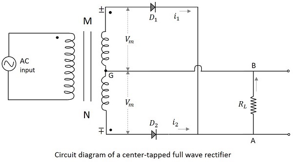
Working of a CT- FWR
The working of a center-tapped full wave rectifier can be understood by the above figure. When the positive half cycle of the input voltage is applied, the point M at the transformer secondary becomes positive with respect to the point N. This makes the diode $D_1$forward biased. Hence current $i_1$ flows through the load resistor from A to B. We now have the positive half cycles in the output
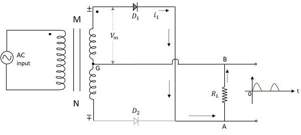
When the negative half cycle of the input voltage is applied, the point M at the transformer secondary becomes negative with respect to the point N. This makes the diode $D_2$ forward biased. Hence current $i_2$ flows through the load resistor from A to B. We now have the positive half cycles in the output, even during the negative half cycles of the input.
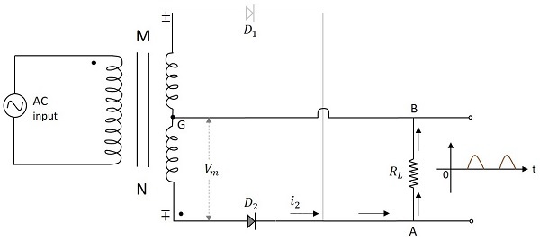
Waveforms of CT FWR
The input and output waveforms of the center-tapped full wave rectifier are as follows.
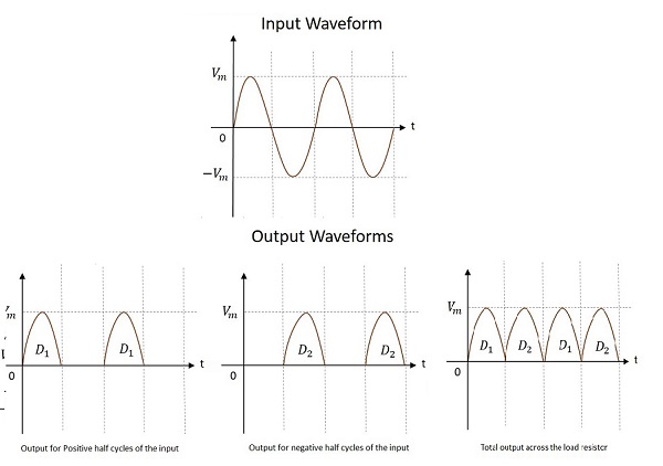
From the above figure it is evident that the output is obtained for both the positive and negative half cycles. It is also observed that the output across the load resistor is in the same direction for both the half cycles.
Peak Inverse Voltage
As the maximum voltage across half secondary winding is $V_m$, the whole of the secondary voltage appears across the non-conducting diode. Hence the peak inverse voltage is twice the maximum voltage across the half-secondary winding, i.e.
$$PIV=2V_m$$
Disadvantages
There are few disadvantages for a center-tapped full wave rectifier such as −
- Location of center-tapping is difficult
- The dc output voltage is small
- PIV of the diodes should be high
The next kind of full wave rectifier circuit is the Bridge Full wave rectifier circuit.
Bridge Full-Wave Rectifier
This is such a full wave rectifier circuit which utilizes four diodes connected in bridge form so as not only to produce the output during the full cycle of input, but also to eliminate the disadvantages of the center-tapped full wave rectifier circuit.
There is no need of any center-tapping of the transformer in this circuit. Four diodes called $D_1$, $D_2$, $D_3$ and $D_4$ are used in constructing a bridge type network so that two of the diodes conduct for one half cycle and two conduct for the other half cycle of the input supply. The circuit of a bridge full wave rectifier is as shown in the following figure.
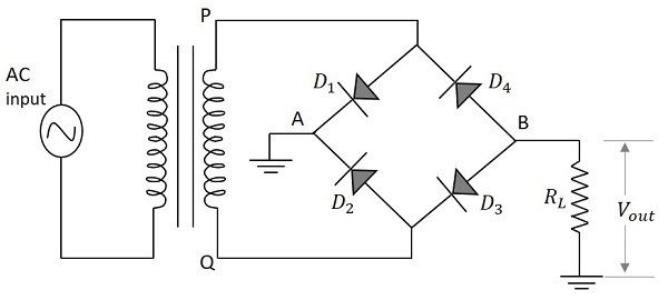
Working of a Bridge Full-Wave Rectifier
The full wave rectifier with four diodes connected in bridge circuit is employed to get a better full wave output response. When the positive half cycle of the input supply is given, point P becomes positive with respect to the point Q. This makes the diode $D_1$ and $D_3$ forward biased while $D_2$ and $D_4$ reverse biased. These two diodes will now be in series with the load resistor.
The following figure indicates this along with the conventional current flow in the circuit.
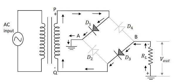
Hence the diodes $D_1$ and $D_3$ conduct during the positive half cycle of the input supply to produce the output along the load resistor. As two diodes work in order to produce the output, the voltage will be twice the output voltage of the center tapped full wave rectifier.
When the negative half cycle of the input supply is given, point P becomes negative with respect to the point Q. This makes the diode $D_1$ and $D_3$ reverse biased while $D_2$ and $D_4$ forward biased. These two diodes will now be in series with the load resistor.
The following figure indicates this along with the conventional current flow in the circuit.
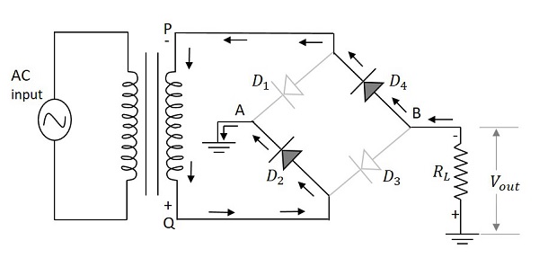
Hence the diodes $D_{2}$ and $D_{4}$ conduct during the negative half cycle of the input supply to produce the output along the load resistor. Here also two diodes work to produce the output voltage. The current flows in the same direction as during the positive half cycle of the input.
Waveforms of Bridge FWR
The input and output waveforms of the center-tapped full wave rectifier are as follows.
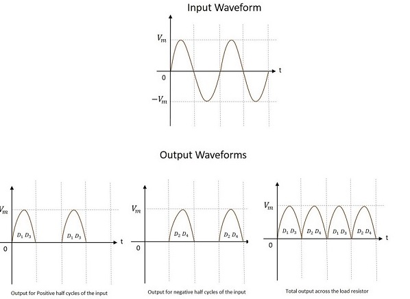
From the above figure, it is evident that the output is obtained for both the positive and negative half cycles. It is also observed that the output across the load resistor is in the same direction for both the half cycles.
Peak Inverse Voltage
Whenever two of the diodes are being in parallel to the secondary of the transformer, the maximum secondary voltage across the transformer appears at the non-conducting diodes which makes the PIV of the rectifier circuit. Hence the peak inverse voltage is the maximum voltage across the secondary winding, i.e.
$$PIV=V_m$$
Advantages
There are many advantages for a bridge full wave rectifier, such as −
- No need of center-tapping.
- The dc output voltage is twice that of the center-tapper FWR.
- PIV of the diodes is of the half value that of the center-tapper FWR.
- The design of the circuit is easier with better output.
Let us now analyze the characteristics of a full-wave rectifier.
Analysis of Full-Wave Rectifier
In order to analyze a full wave rectifier circuit, let us assume the input voltage $V_{i}$ as,
$$V_{i}=V_m \sin \omega t$$
The current $i_1$ through the load resistor $R_L$ is given by
$$i_1=I_m \sin \omega t \quad for \quad0 \leq \omega t \leq \pi$$
$$i_1=\quad0 \quad\quad\quad for \quad \pi \leq \omega t \leq 2\pi$$
Where
$$I_m=\frac{V_m}{R_f+R_L}$$
$R_f$ being the diode resistance in ON condition.
Similarly, the current $i_2$ flowing through diode $D_2$ and load resistor RL is given by,
$$i_2=\quad\:0 \quad\quad\quad for \quad 0 \leq \omega t \leq \pi$$
$$i_2=I_m \sin \omega t \quad for \quad\pi \leq \omega t \leq 2\pi$$
The total current flowing through $R_L$ is the sum of the two currents $i_1$ and $i_2$ i.e.
$$i=i_1+i_2$$
D.C. or Average Current
The average value of output current that a D.C. ammeter will indicate is given by
$$I_{dc}=\frac{1}{2\pi} \int_{0}^{2\pi} i_1 \:d\left ( \omega t \right )+\frac{1}{2\pi}\int_{0}^{2\pi}i_2 \:d\left ( \omega t \right )$$
$$=\frac{1}{2\pi\int_{0}^{\pi}}I_m \sin \omega t \:d\left ( \omega t \right )+0+0+$$
$$\frac{1}{2\pi} \int_{0}^{2\pi}I_m \sin \omega t\:d\left ( \omega t \right ) $$
$$=\frac{I_m}{\pi}+ \frac{I_m}{\pi} =\frac{2I_m}{\pi}=0.636I_m$$
This is double the value of a half wave rectifier.
D.C. Output Voltage
The dc output voltage across load is given by
$$V_{dc}=I_{dc}\times R_L = \frac{2I_mR_L}{\pi}=0.636I_mR_L$$
Thus the dc output voltage is twice that of a half wave rectifier.
RMS Current
The RMS value of the current is given by
$$I_{rms}=\left [ \frac{1}{\pi}\int_{0}^{\pi} t^2 \:d\left ( \omega t \right )\right ]^{\frac{1}{2}}$$
Since current is of the two same form in the two halves
$$=\left [ \frac{I_{m}^{2}}{\pi} \int_{0}^{\pi }\sin^2 \omega t\:d\left ( \omega t \right )\right ]^{\frac{1}{2}}$$
$$=\frac{I_m}{\sqrt{2}}$$
Rectifier Efficiency
The rectifier efficiency is defined as
$$\eta=\frac{P_{dc}}{P_{ac}}$$
Now,
$$P_{dc}=\left (V_{dc} \right )^2/R_L=\left ( 2V_m/\pi \right )^2$$
And,
$$P_{ac}=\left (V_{rms} \right )^2/R_L=\left (V_m/\sqrt{2} \right )^2$$
Therefore,
$$\eta =\frac{P_{dc}}{P_{ac}}=\frac{\left (2V_m/\pi \right )^2}{\left ( V_m/\sqrt{2} \right )^2}=\frac{8}{\pi^2}$$
$$=0.812=81.2\%$$
The rectifier efficiency can be calculated as follows −
The dc output power,
$$P_{dc}=I_{dc}^{2}R_L=\frac{4I_{m}^{2}}{\pi^2}\times R_L$$
The ac input power,
$$P_{ac}=I_{rms}^{2}\left (R_f+R_L \right )=\frac{I_{m}^{2}}{2}\left ( R_f+R_L \right )$$
Therefore,
$$\eta=\frac{4I_{m}^{2}R_L/\pi^2}{I_{m}^{2}\left ( R_f+R_L \right )/2}=\frac{8}{\pi^2}\frac{R_L}{\left ( R_f+R_L \right )}$$
$$=\frac{0.812}{\left \{ 1+\left ( R_f/R_L \right ) \right \}}$$
Therefore, Percentage Efficiency is
$$=\frac{0.812}{ 1+\left ( R_f+R_L \right )}$$
$$=81.2\% \quad if\: R_f=0$$
Thus, a full-wave rectifier has efficiency twice that of half wave rectifier.
Ripple Factor
The form factor of rectified output voltage of a full wave rectifier is given by
$$F=\frac{I_{rms}}{I_{dc}}=\frac{I_m/\sqrt{2}}{2I_m/\pi}=1.11$$
The ripple factor $\gamma$ is defined as (using ac circuit theory)
$$\gamma =\left [ \left ( \frac{I_{rms}}{I_{dc}} \right )-1 \right ]^{\frac{1}{2}}=\left ( F^2 -1\right )^{\frac{1}{2}}$$
$$=\left [ \left ( 1.11 \right )^2 -1\right ]^\frac{1}{2}=0.48$$
This is a great improvement over the half wave rectifiers ripple factor which was 1.21
Regulation
The dc output voltage is given by
$$V_{dc}=\frac{2I_mR_L}{\pi}=\frac{2V_mR_L}{\pi\left ( R_f+R_L \right )}$$
$$=\frac{2V_m}{\pi}\left [ 1-\frac{R_f}{R_f+R_L} \right ]=\frac{2V_m}{\pi}-I_{dc}R_f$$
Transformer Utilization Factor
The TUF of a half wave rectifier is 0.287
There are two secondary windings in a center-tapped rectifier and hence the TUF of centertapped full wave rectifier is
$$\left ( TUF \right )_{avg}=\frac{P_{dc}}{V-A\:rating\:of\:a\:transformer}$$
$$=\frac{\left ( TUF \right )_p+\left ( TUF \right )_s+\left ( TUF \right )_s}{3}$$
$$=\frac{0.812+0.287+0.287}{3}=0.693$$
Half-Wave vs. Full-Wave Rectifier
After having gone through all the values of different parameters of the full wave rectifier, let us just try to compare and contrast the features of half-wave and full-wave rectifiers.
| Terms | Half Wave Rectifier | Center Tapped FWR | Bridge FWR |
|---|---|---|---|
| Number of Diodes | $1$ | $2$ | $4$ |
| Transformer tapping | $No$ | $Yes$ | $No$ |
| Peak Inverse Voltage | $V_m$ | $2V_m$ | $V_m$ |
| Maximum Efficiency | $40.6\%$ | $81.2\%$ | $81.2\%$ |
| Average / dc current | $I_m/\pi$ | $2I_m/\pi$ | $2I_m/\pi$ |
| DC voltage | $V_m/\pi$ | $2V_m/\pi$ | $2V_m/\pi$ |
| RMS current | $I_m/2$ | $I_m/\sqrt{2}$ | $I_m/\sqrt{2}$ |
| Ripple Factor | $1.21$ | $0.48$ | $0.48$ |
| Output frequency | $f_{in}$ | $2f_{in}$ | $2f_{in}$ |
Electronic Circuits - Filters
The power supply block diagram clearly explains that a filter circuit is needed after the rectifier circuit. A rectifier helps in converting a pulsating alternating current to direct current, which flows only in one direction. Till now, we have seen different types of rectifier circuits.
The outputs of all these rectifier circuits contains some ripple factor. We have also observed that the ripple factor of a half wave rectifier is greater than that of a full wave rectifier.
Why Do We Need Filters?
The ripple in the signal denotes the presence of some AC component. This ac component has to be completely removed in order to get pure dc output. So, we need a circuit that smoothens the rectified output into a pure dc signal.
A filter circuit is one which removes the ac component present in the rectified output and allows the dc component to reach the load.
The following figure shows the functionality of a filter circuit.
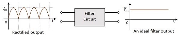
A filter circuit is constructed using two main components, inductor and capacitor. We have already studied in Basic Electronics tutorial that
An inductor allows dc and blocks ac.
A capacitor allows ac and blocks dc.
Let us try to construct a few filters, using these two components.
Series Inductor Filter
As an inductor allows dc and blocks ac, a filter called Series Inductor Filter can be constructed by connecting the inductor in series, between the rectifier and the load. The figure below shows the circuit of a series inductor filter.
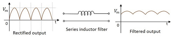
The rectified output when passed through this filter, the inductor blocks the ac components that are present in the signal, in order to provide a pure dc. This is a simple primary filter.
Shunt Capacitor Filter
As a capacitor allows ac through it and blocks dc, a filter called Shunt Capacitor Filter can be constructed using a capacitor, connected in shunt, as shown in the following figure.
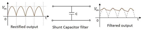
The rectified output when passed through this filter, the ac components present in the signal are grounded through the capacitor which allows ac components. The remaining dc components present in the signal are collected at the output.
The above filter types discussed are constructed using an inductor or a capacitor. Now, lets try to use both of them to make a better filter. These are combinational filters.
L-C Filter
A filter circuit can be constructed using both inductor and capacitor in order to obtain a better output where the efficiencies of both inductor and capacitor can be used. The figure below shows the circuit diagram of a LC filter.
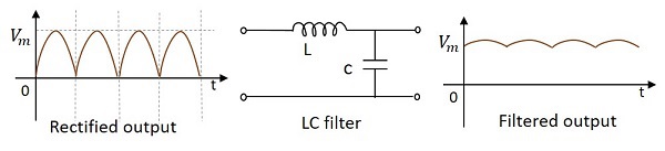
The rectified output when given to this circuit, the inductor allows dc components to pass through it, blocking the ac components in the signal. Now, from that signal, few more ac components if any present are grounded so that we get a pure dc output.
This filter is also called as a Choke Input Filter as the input signal first enters the inductor. The output of this filter is a better one than the previous ones.
Π- Filter (Pi filter)
This is another type of filter circuit which is very commonly used. It has capacitor at its input and hence it is also called as a Capacitor Input Filter. Here, two capacitors and one inductor are connected in the form of shaped network. A capacitor in parallel, then an inductor in series, followed by another capacitor in parallel makes this circuit.
If needed, several identical sections can also be added to this, according to the requirement. The figure below shows a circuit for $\pi$ filter (Pi-filter).
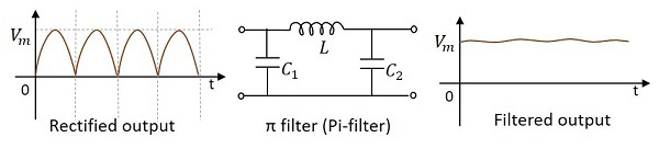
Working of a Pi filter
In this circuit, we have a capacitor in parallel, then an inductor in series, followed by another capacitor in parallel.
Capacitor C1 − This filter capacitor offers high reactance to dc and low reactance to ac signal. After grounding the ac components present in the signal, the signal passes to the inductor for further filtration.
Inductor L − This inductor offers low reactance to dc components, while blocking the ac components if any got managed to pass, through the capacitor C1.
Capacitor C2 − Now the signal is further smoothened using this capacitor so that it allows any ac component present in the signal, which the inductor has failed to block.
Thus we, get the desired pure dc output at the load.
Electronic Circuits - Regulators
The next and the last stage before load, in a power supply system is the Regulator part. Let us now try to understand what a regulator is and what it does.
The part of electronics that deal with the control and conversion of electric power can be termed as Power Electronics. A regulator is an important device when it comes to power electronics as it controls the power output.
Need for a Regulator
For a Power supply to produce a constant output voltage, irrespective of the input voltage variations or the load current variations, there is a need for a voltage regulator.
A voltage regulator is such a device that maintains constant output voltage, instead of any kind of fluctuations in the input voltage being applied or any variations in current, drawn by the load. The following image gives an idea of what a practical regulator looks like.
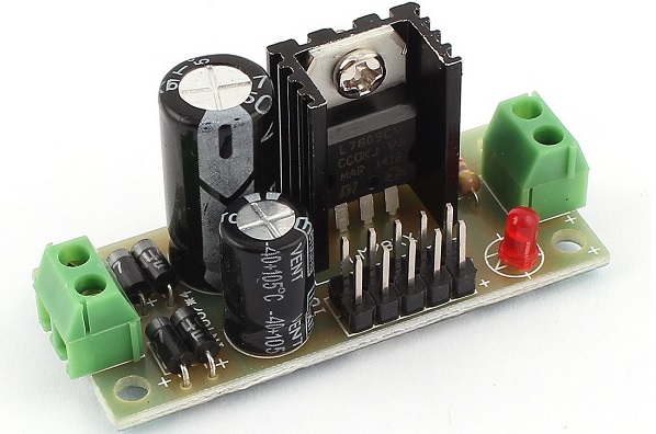
Types of Regulators
Regulators can be classified into different categories, depending upon their working and type of connection.
Depending upon the type of regulation, the regulators are mainly divided into two types namely, line and load regulators.
Line Regulator − The regulator which regulates the output voltage to be constant, in spite of input line variations, it is called as Line regulator.
Load Regulator − The regulator which regulates the output voltage to be constant, in spite of the variations in load at the output, it is called as Load regulator.
Depending upon the type of connection, there are two type of voltage regulators. They are
- Series voltage regulator
- Shunt voltage regulator
The arrangement of them in a circuit will be just as in the following figures.
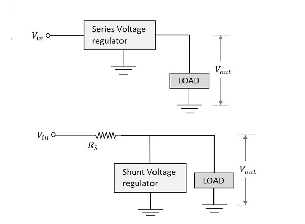
Let us have a look at other important regulator types.
Zener Voltage Regulator
A Zener voltage regulator is one which uses Zener diode for regulating the output voltage. We have already discussed the details regarding Zener diode in BASIC ELECTRONICS tutorial.
When the Zener diode is operated in the breakdown or Zener region, the voltage across it is substantially constant for a large change of current through it. This characteristic makes Zener diode a good voltage regulator.
The following figure shows an image of a simple Zener regulator.
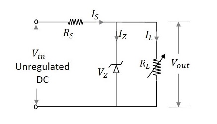
The applied input voltage $V_i$ when increased beyond the Zener voltage $V_z$, then the Zener diode operates in the breakdown region and maintains constant voltage across the load. The series limiting resistor $R_s$ limits the input current.
Working of Zener Voltage Regulator
The Zener diode maintains the voltage across it constant in spite of load variations and input voltage fluctuations. Hence we can consider 4 cases to understand the working of a Zener voltage regulator.
Case 1 − If the load current $I_L$ increases, then the current through the Zener diode $I_Z$ decreases in order to maintain the current through the series resistor $R_S$ constant. The output voltage Vo depends upon the input voltage Vi and voltage across the series resistor $R_S$.
This is can be written as
$$V_o=V_{in}-IR_{s}$$
Where $I$ is constant. Therefore, $V_o$ also remains constant.
Case 2 − If the load current $I_L$ decreases, then the current through the Zener diode $I_Z$ increases, as the current $I_S$ through RS series resistor remains constant. Though the current $I_Z$ through Zener diode increases it maintains a constant output voltage $V_Z$, which maintains the load voltage constant.
Case 3 − If the input voltage $V_i$ increases, then the current $I_S$ through the series resistor RS increases. This increases the voltage drop across the resistor, i.e. $V_S$ increases. Though the current through Zener diode $I_Z$ increases with this, the voltage across Zener diode $V_Z$ remains constant, keeping the output load voltage constant.
Case 4 − If the input voltage decreases, the current through the series resistor decreases which makes the current through Zener diode $I_Z$ decreases. But the Zener diode maintains output voltage constant due to its property.
Limitations of Zener Voltage Regulator
There are a few limitations for a Zener voltage regulator. They are −
- It is less efficient for heavy load currents.
- The Zener impedance slightly affects the output voltage.
Hence a Zener voltage regulator is considered effective for low voltage applications. Now, let us go through the other types of voltage regulators, which are made using transistors.
Transistor Series Voltage Regulator
This regulator has a transistor in series to the Zener regulator and both in parallel to the load. The transistor works as a variable resistor regulating its collector emitter voltage in order to maintain the output voltage constant. The figure below shows the transistor series voltage regulator.
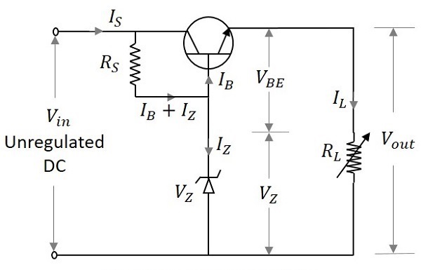
With the input operating conditions, the current through the base of the transistor changes. This effects the voltage across the base emitter junction of the transistor $V_{BE}$. The output voltage is maintained by the Zener voltage $V_Z$ which is constant. As both of them are maintained equal, any change in the input supply is indicated by the change in emitter base voltage $V_{BE}$.
Hence the output voltage Vo can be understood as
$$V_O=V_Z+V_{BE}$$
Working of Transistor Series Voltage Regulator
The working of a series voltage regulator shall be considered for input and load variations. If the input voltage is increased, the output voltage also increases. But this in turn makes the voltage across the collector base junction $V_{BE}$ to decrease, as the Zener voltage $V_Z$ remains constant. The conduction decreases as the resistance across emitter collector region increases. This further increases the voltage across collector emitter junction VCE thus reducing the output voltage $V_O$. This will be similar when the input voltage decreases.
When the load changes occur, which means if the resistance of the load decreases, increasing the load current $I_L$, the output voltage $V_O$ decreases, increasing the emitter base voltage $V_{BE}$.
With the increase in the emitter base voltage $V_{BE}$ the conduction increases reducing the emitter collector resistance. This in turn increases the input current which compensates the decrease in the load resistance. This will be similar when the load current increases.
Limitations of Transistor Series Voltage Regulator
Transistor Series Voltage Regulators have the following limitations −
- The voltages $V_{BE}$ and $V_Z$ are affected by the rise in temperature.
- No good regulation for high currents is possible.
- Power dissipation is high.
- Power dissipation is high.
- Less efficient.
To minimize these limitations, transistor shunt regulator is used.
Transistor Shunt Voltage Regulator
A transistor shunt regulator circuit is formed by connecting a resistor in series with the input and a transistor whose base and collector are connected by a Zener diode that regulates, both in parallel with the load. The figure below shows the circuit diagram of a transistor shunt regulator.
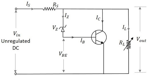
Working of Transistor Shunt Voltage Regulator
If the input voltage increases, the $V_{BE}$ and $V_O$ also gets increased. But this happens initially. Actually when $V_{in}$ increases, the current $I_{in}$ also increases. This current when flows through RS, causes a voltage drop $V_S$ across the series resistor, which also gets increased with $V_{in}$. But this makes $V_o$ to decrease. Now this decrease in $V_o$ compensates the initial increase maintaining it to be constant. Hence $V_o$ is maintained constant. If the output voltage decreases instead, the reverse happens.
If the load resistance decreases, there should be decrease in the output voltage $V_o$. The current through the load increases. This makes the base current and collector current of the transistor to decrease. The voltage across the series resistor becomes low, as the current flows heavily. The input current will be constant.
The output voltage appears will be the difference between the applied voltage $V_i$ and the series voltage drop $V_s$. Hence the output voltage will be increased to compensate the initial decrease and hence maintained constant. The reverse happens if the load resistance increases.
IC Regulators
Voltage Regulators are now-a-days available in the form of Integrated Circuits (ICs). These are in short called as IC Regulators.
Along with the functionality like a normal regulator, an IC regulator has the properties like thermal compensation, short circuit protection and surge protection which are built into the device.
Types of IC regulators
IC regulators can be of the following types −
- Fixed Positive voltage regulators
- Fixed Negative voltage regulators
- Adjustable voltage regulators
- Dual-tracking voltage regulators
Let us now discuss them in detail.
Fixed Positive Voltage Regulator
The output of these regulators is fixed to a specific value and the values are positive, which means the output voltage provided is positive voltage.
The most used series is 7800 series and the ICs will be like IC 7806, IC 7812 and IC 7815 etc. which provide +6v, +12v and +15v respectively as output voltages. The figure below shows the IC 7810 connected to provide a fixed 10v positive regulated output voltage.
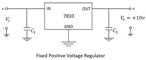
In the above figure, the input capacitor $C_1$ is used to prevent unwanted oscillations and the output capacitor $C_2$ acts as a line filter to improve transient response.
Fixed Negative Voltage Regulator
The output of these regulators is fixed to a specific value and the values are negative, which means the output voltage provided is negative voltage.
The most used series is 7900 series and the ICs will be like IC 7906, IC 7912 and IC 7915 etc. which provide -6v, -12v and -15v respectively as output voltages. The figure below shows the IC 7910 connected to provide a fixed 10v negative regulated output voltage.
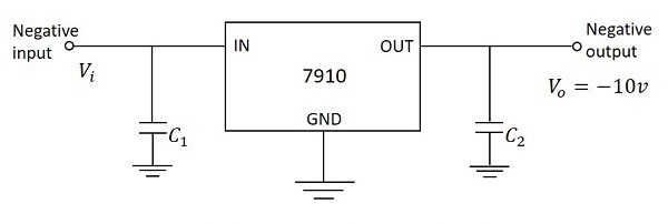
In the above figure, the input capacitor $C_1$ is used to prevent unwanted oscillations and the output capacitor $C_2$ acts as a line filter to improve transient response.
Adjustable Voltage Regulators
An adjustable voltage regulator has three terminals IN, OUT and ADJ. The input and output terminals are common whereas the adjustable terminal is provided with a variable resistor which lets the output to vary between a wide range.
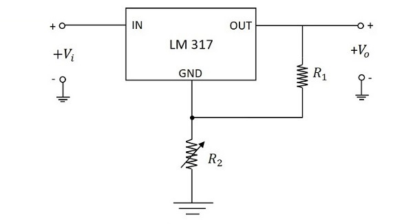
The above figure shows an unregulated power supply driving a LM 317 adjustable IC regulator which is commonly used. The LM 317 is a three terminal positive adjustable voltage regulator and can supply 1.5A of load current over an adjustable output range of 1.25v to 37v.
Dual-Tracking Voltage Regulators
A dual-tracking regulator is used when split-supply voltages are needed. These provide equal positive and negative output voltages. For example, the RC4195 IC provides D.C. outputs of +15v and -15v. This needs two unregulated input voltages such as the positive input may vary from +18v to +30v and negative input may vary from -18v to -30v.
The above image shows a dual-tracking RC4195 IC regulator. The adjustable dual-tacking regulators are also available whose outputs vary between two rated limits.
Electronic Circuits - SMPS
The topics discussed till now represent different sections of power supply unit. All these sections together make the Linear Power Supply. This is the conventional method of obtaining DC out of the input AC supply.
Linear Power Supply
The Linear Power Supply (LPS) is the regulated power supply which dissipates much heat in the series resistor to regulate the output voltage which has low ripple and low noise. This LPS has many applications.
A linear power supply requires larger semiconductor devices to regulate the output voltage and generates more heat resulting in lower energy efficiency. Linear power supplies have transient response times up to 100 times faster than the others, which is very important in certain specialized areas.
Advantages of LPS
- The power supply is continuous.
- The circuitry is simple.
- These are reliable systems.
- This system dynamically responds to load changes.
- The circuit resistances are changed to regulate the output voltage.
- As the components operate in linear region, the noise is low.
- The ripple is very low in the output voltage.
Disadvantages of LPS
- The transformers used are heavier and large.
- The heat dissipation is more.
- The efficiency of linear power supply is 40 to 50%
- Power is wasted in the form of heat in LPS circuits.
- Single output voltage is obtained.
We have already gone through different parts of a Linear Power supply. The block diagram of a Linear Power Supply is as shown in the following figure.
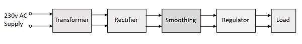
In spite of the above disadvantages, Linear Power Supplies are widely used in low-noise amplifiers, test equipment, control circuits. In addition, they are also used in data acquisition and signal processing.
All the power supply systems that needs simple regulation and where efficiency is not a concern, the LPS circuits are used. As the electrical noise is lower, the LPS is used in powering sensitive analog circuitry. But to overcome the disadvantages of Linear Power Supply system, the Switched Mode Power Supply (SMPS) is used.
Switched Mode Power Supply (SMPS)
The disadvantages of LPS such as lower efficiency, the need for large value of capacitors to reduce ripples and heavy and costly transformers etc. are overcome by the implementation of Switched Mode Power Supplies.
The working of SMPS is simply understood by knowing that the transistor used in LPS is used to control the voltage drop while the transistor in SMPS is used as a controlled switch.
Working
The working of SMPS can be understood by the following figure.
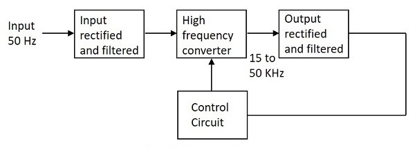
Let us try to understand what happens at each stage of SMPS circuit.
Input Stage
The AC input supply signal 50 Hz is given directly to the rectifier and filter circuit combination without using any transformer. This output will have many variations and the capacitance value of the capacitor should be higher to handle the input fluctuations. This unregulated dc is given to the central switching section of SMPS.
Switching Section
A fast switching device such as a Power transistor or a MOSFET is employed in this section, which switches ON and OFF according to the variations and this output is given to the primary of the transformer present in this section. The transformer used here are much smaller and lighter ones unlike the ones used for 60 Hz supply. These are much efficient and hence the power conversion ratio is higher.
Output Stage
The output signal from the switching section is again rectified and filtered, to get the required DC voltage. This is a regulated output voltage which is then given to the control circuit, which is a feedback circuit. The final output is obtained after considering the feedback signal.
Control Unit
This unit is the feedback circuit which has many sections. Let us have a clear understanding about this from The following figure.
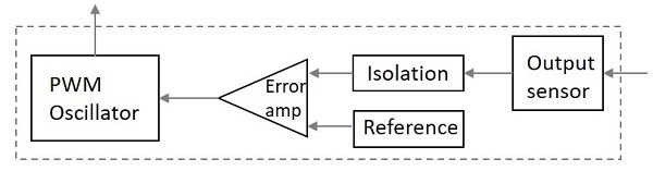
The above figure explains the inner parts of a control unit. The output sensor senses the signal and joins it to the control unit. The signal is isolated from the other section so that any sudden spikes should not affect the circuitry. A reference voltage is given as one input along with the signal to the error amplifier which is a comparator that compares the signal with the required signal level.
By controlling the chopping frequency the final voltage level is maintained. This is controlled by comparing the inputs given to the error amplifier, whose output helps to decide whether to increase or decrease the chopping frequency. The PWM oscillator produces a standard PWM wave fixed frequency.
We can get a better idea on the complete functioning of SMPS by having a look at the following figure.
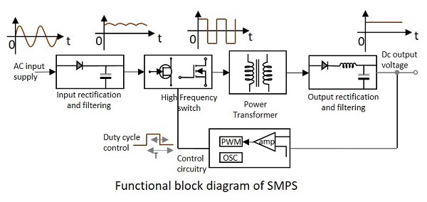
The SMPS is mostly used where switching of voltages is not at all a problem and where efficiency of the system really matters. There are few points which are to be noted regarding SMPS. They are
SMPS circuit is operated by switching and hence the voltages vary continuously.
The switching device is operated in saturation or cut off mode.
The output voltage is controlled by the switching time of the feedback circuitry.
Switching time is adjusted by adjusting the duty cycle.
The efficiency of SMPS is high because, instead of dissipating excess power as heat, it continuously switches its input to control the output.
Disadvantages
There are few disadvantages in SMPS, such as
- The noise is present due to high frequency switching.
- The circuit is complex.
- It produces electromagnetic interference.
Advantages
The advantages of SMPS include,
- The efficiency is as high as 80 to 90%
- Less heat generation; less power wastage.
- Reduced harmonic feedback into the supply mains.
- The device is compact and small in size.
- The manufacturing cost is reduced.
- Provision for providing the required number of voltages.
Applications
There are many applications of SMPS. They are used in the motherboard of computers, mobile phone chargers, HVDC measurements, battery chargers, central power distribution, motor vehicles, consumer electronics, laptops, security systems, space stations, etc.
Types of SMPS
SMPS is the Switched Mode Power Supply circuit which is designed for obtaining the regulated DC output voltage from an unregulated DC or AC voltage. There are four main types of SMPS such as
- DC to DC Converter
- AC to DC Converter
- Fly back Converter
- Forward Converter
The AC to DC conversion part in the input section makes the difference between AC to DC converter and DC to DC converter. The Fly back converter is used for Low power applications. Also there are Buck Converter and Boost converter in the SMPS types which decrease or increase the output voltage depending upon the requirements. The other type of SMPS include Self-oscillating fly-back converter, Buck-boost converter, Cuk, Sepic, etc.