- Linear Wave Shapping
- Special Functions of LPF and HPF
- Nonlinear Wave Shapping
- Positive Clipper Circuits
- Negative Clipper Circuits
- Clamper Circuits
- Limiter & Voltage Multiplier
- Diode as a Switch
- Power Supplies
- Power Supplies
- Electronic Circuits - Rectifiers
- Full Wave Rectifiers
- Electronic Circuits - Filters
- Electronic Circuits - Regulators
- Electronic Circuits - SMPS
- Electronic Circuits Resources
- Electronic Circuits - Quick Guide
- Electronic Circuits - Resources
- Electronic Circuits - Discussion
Electronic Circuits - Diode as a Switch
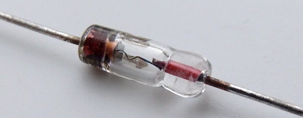
Diode is a two terminal PN junction that can be used in various applications. One of such applications is an electrical switch. The PN junction, when forward biased acts as close circuited and when reverse biased acts as open circuited. Hence the change of forward and reverse biased states makes the diode work as a switch, the forward being ON and the reverse being OFF state.
Electrical Switches over Mechanical Switches
Electrical switches are a preferred choice over mechanical switches due to the following reasons −
- Mechanical switches are prone to oxidation of metals whereas electrical switches dont.
- Mechanical switches have movable contacts.
- They are more prone to stress and strain than electrical switches.
- The worn and torn of mechanical switches often affect their working.
Hence an electrical switch is more useful than a Mechanical switch.
Working of Diode as a Switch
Whenever a specified voltage is exceeded, the diode resistance gets increased, making the diode reverse biased and it acts as an open switch. Whenever the voltage applied is below the reference voltage, the diode resistance gets decreased, making the diode forward biased, and it acts as a closed switch.
The following circuit explains the diode acting as a switch.
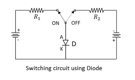
A switching diode has a PN junction in which P-region is lightly doped and N-region is heavily doped. The above circuit symbolizes that the diode gets ON when positive voltage forward biases the diode and it gets OFF when negative voltage reverse biases the diode.
Ringing
As the forward current flows till then, with a sudden reverse voltage, the reverse current flows for an instance rather than getting switched OFF immediately. The higher the leakage current, the greater the loss. The flow of reverse current when diode is reverse biased suddenly, may sometimes create few oscillations, called as RINGING.
This ringing condition is a loss and hence should be minimized. To do this, the switching times of the diode should be understood.
Diode Switching Times
While changing the bias conditions, the diode undergoes a transient response. The response of a system to any sudden change from an equilibrium position is called as transient response.
The sudden change from forward to reverse and from reverse to forward bias, affects the circuit. The time taken to respond to such sudden changes is the important criterion to define the effectiveness of an electrical switch.
The time taken before the diode recovers its steady state is called as Recovery Time.
The time interval taken by the diode to switch from reverse biased state to forward biased state is called as Forward Recovery Time.($t_{fr}$)
The time interval taken by the diode to switch from forward biased state to reverse biased state is called as Reverse Recovery Time. ($t_{fr}$)
To understand this more clearly, let us try to analyze what happens once the voltage is applied to a switching PN diode.
Carrier Concentration
Minority charge carrier concentration reduces exponentially as seen away from the junction. When the voltage is applied, due to the forward biased condition, the majority carriers of one side move towards the other. They become minority carriers of the other side. This concentration will be more at the junction.
For example, if N-type is considered, the excess of holes that enter into N-type after applying forward bias, adds to the already present minority carriers of N-type material.
Let us consider few notations.
- The majority carriers in P-type (holes) = $P_{po}$
- The majority carriers in N-type (electrons) = $N_{no}$
- The minority carriers in P-type (electrons) = $N_{po}$
- The majority carriers in N-type (holes) = $P_{no}$
During Forward biased Condition − The minority carriers are more near junction and less far away from the junction. The graph below explains this.
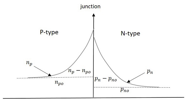
Excess minority carrier charge in P-type = $P_n-P_{no}$ with $p_{no}$ (steady state value)
Excess minority carrier charge in N-type = $N_p-N_{po}$ with $N_{po}$ (steady state value)
During reverse bias condition − Majority carriers doesnt conduct the current through the junction and hence dont participate in current condition. The switching diode behaves as a short circuited for an instance in reverse direction.
The minority carriers will cross the junction and conduct the current, which is called as Reverse Saturation Current. The following graph represents the condition during reverse bias.
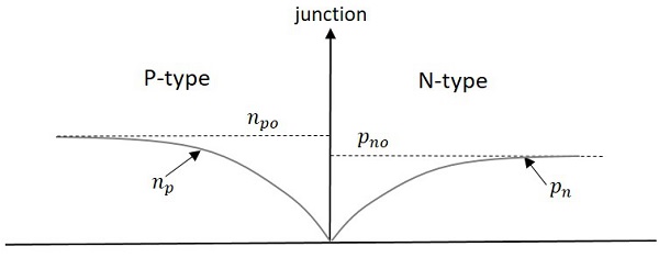
In the above figure, the dotted line represents equilibrium values and solid lines represent actual values. As the current due to minority charge carriers is large enough to conduct, the circuit will be ON until this excess charge is removed.
The time required for the diode to change from forward bias to reverse bias is called Reverse recovery time ($t_{rr}$). The following graphs explain the diode switching times in detail.
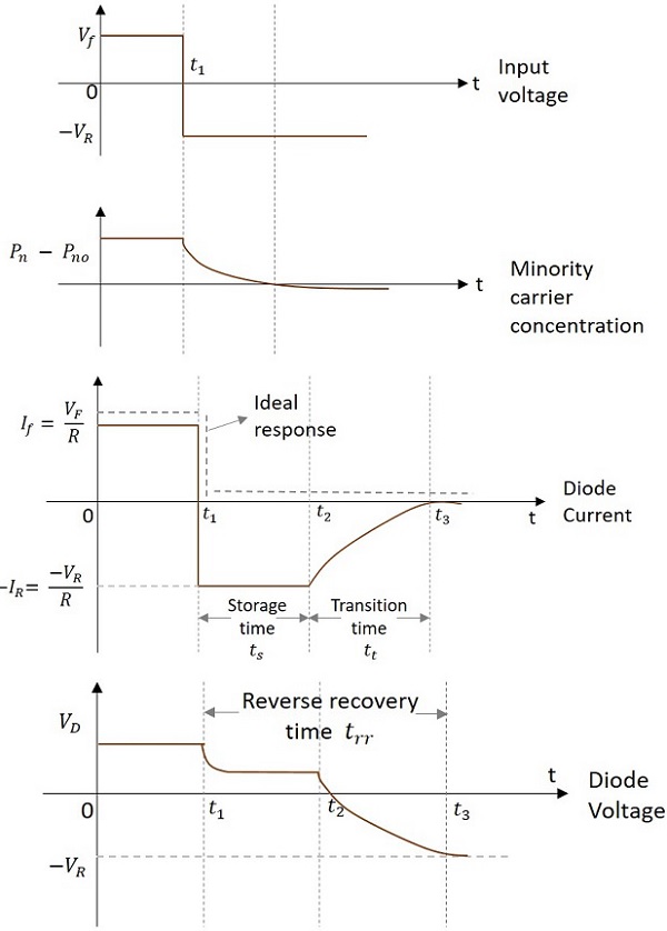
From the above figure, let us consider the diode current graph.
At $t_{1}$ the diode is suddenly brought to OFF state from ON state; it is known as Storage time. Storage time is the time required to remove the excess minority carrier charge. The negative current flowing from N to P type material is of a considerable amount during the Storage time. This negative current is,
$$-I_R= \frac{-V_{R}}{R}$$
The next time period is the transition time (from $t_2$ to $t_3$)
Transition time is the time taken for the diode to get completely to open circuit condition. After $t_3$ diode will be in steady state reverse bias condition. Before $t_1$ diode is under steady state forward bias condition.
So, the time taken to get completely to open circuit condition is
$$Reverse \:\:recovery\:\: time\left ( t_{rr} \right )= Storage \:\:time \left ( T_{s} \right )+Transition \:\: time \left ( T_{t} \right )$$
Whereas to get to ON condition from OFF, it takes less time called as Forward recovery time. Reverse recovery time is greater than Forward recovery time. A diode works as a better switch if this Reverse recovery time is made less.
Definitions
Let us just go through the definitions of the time periods discussed.
Storage time − The time period for which the diode remains in the conduction state even in the reverse biased state, is called as Storage time.
Transition time − The time elapsed in returning back to the state of non-conduction, i.e. steady state reverse bias, is called Transition time.
Reverse recovery time − The time required for the diode to change from forward bias to reverse bias is called as Reverse recovery time.
Forward recovery time − The time required for the diode to change from reverse bias to forward bias is called as Forward recovery time.
Factors that affect diode switching times
There are few factors that affect the diode switching times, such as
Diode Capacitance − The PN junction capacitance changes depending upon the bias conditions.
Diode Resistance − The resistance offered by the diode to change its state.
Doping Concentration − The level of doping of the diode, affects the diode switching times.
Depletion Width − The narrower the width of the depletion layer, the faster the switching will be. A Zener diode has narrow depletion region than an avalanche diode, which makes the former a better switch.
Applications
There are many applications in which diode switching circuits are used, such as −
- High speed rectifying circuits
- High speed switching circuits
- RF receivers
- General purpose applications
- Consumer applications
- Automotive applications
- Telecom applications etc.