- Pulse Circuits Time Base Generators
- Time Base Generators (Overview)
- Types of Time Base Generators
- Bootstrap Time Base Generator
- Miller Sweep Generator
- Pulse Circuits Sweep Circuits
- Unijunction Transistor
- UJT as Relaxation Oscillator
- Pulse Circuits - Synchronization
- Pulse Circuits - Blocking Oscillators
- Pulse Circuits Sampling Gates
- Pulse Circuits - Sampling Gates
- Unidirectional Sampling Gate
- Unidirectional with More Inputs
- Bidirectional Sampling Gates
- Pulse Circuits Useful Resources
- Pulse Circuits - Quick Guide
- Pulse Circuits - Useful Resources
- Pulse Circuits - Discussion
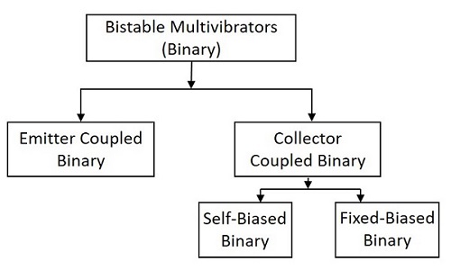
Pulse Circuits - Bistable Multivibrator
A Bistable Multivibrator has two stable states. The circuit stays in any one of the two stable states. It continues in that state, unless an external trigger pulse is given. This Multivibrator is also known as Flip-flop. This circuit is simply called as Binary.
There are few types in Bistable Multivibrators. They are as shown in the following figure.
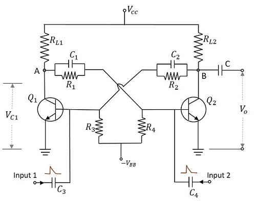
Construction of Bistable Multivibrator
Two similar transistors Q1 and Q2 with load resistors RL1 and RL2 are connected in feedback to one another. The base resistors R3 and R4 are joined to a common source VBB. The feedback resistors R1 and R2 are shunted by capacitors C1 and C2 known as Commutating Capacitors. The transistor Q1 is given a trigger input at the base through the capacitor C3 and the transistor Q2 is given a trigger input at its base through the capacitor C4.
The capacitors C1 and C2 are also known as Speed-up Capacitors, as they reduce the transition time, which means the time taken for the transfer of conduction from one transistor to the other.
The following figure shows the circuit diagram of a self-biased Bistable Multivibrator.
Operation of Bistable Multivibrator
When the circuit is switched ON, due to some circuit imbalances as in Astable, one of the transistors, say Q1 gets switched ON, while the transistor Q2 gets switched OFF. This is a stable state of the Bistable Multivibrator.
By applying a negative trigger at the base of transistor Q1 or by applying a positive trigger pulse at the base of transistor Q2, this stable state is unaltered. So, let us understand this by considering a negative pulse at the base of transistor Q1. As a result, the collector voltage increases, which forward biases the transistor Q2. The collector current of Q2 as applied at the base of Q1, reverse biases Q1 and this cumulative action, makes the transistor Q1 OFF and transistor Q2 ON. This is another stable state of the Multivibrator.
Now, if this stable state has to be changed again, then either a negative trigger pulse at transistor Q2 or a positive trigger pulse at transistor Q1 is applied.
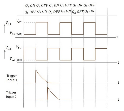
Output Waveforms
The output waveforms at the collectors of Q1 and Q2 along with the trigger inputs given at the bases of QW and Q2 are shown in the following figures.
Advantages
The advantages of using a Bistable Multivibrator are as follows −
- Stores the previous output unless disturbed.
- Circuit design is simple
Disadvantages
The drawbacks of a Bistable Multivibrator are as follows −
- Two kinds of trigger pulses are required.
- A bit costlier than other Multivibrators.
Applications
Bistable Multivibrators are used in applications such as pulse generation and digital operations like counting and storing of binary information.
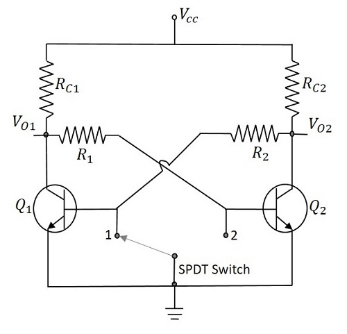
Fixed-bias Binary
A fixed-bias binary circuit is similar to an Astable Multivibrator but with a simple SPDT switch. Two transistors are connected in feedback with two resistors, having one collector connected to the base of the other. The figure below shows the circuit diagram of a fixed-bias binary.
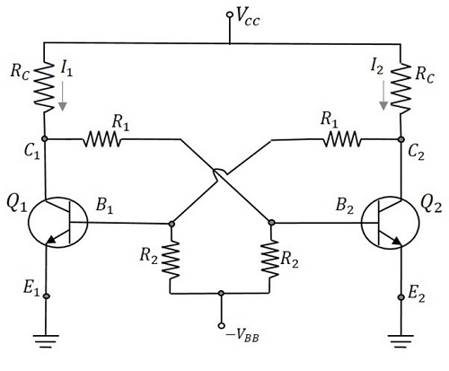
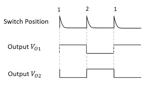
To understand the operation, let us consider the switch to be in position 1. Now the transistor Q1 will be OFF as the base is grounded. The collector voltage at the output terminal VO1 will be equal to VCC which turns the transistor Q2 ON. The output at the terminal VO2 goes LOW. This is a stable state which can be altered only by an external trigger. The change of switch to position 2, works as a trigger.
When the switch is altered, the base of transistor Q2 is grounded turning it to OFF state. The collector voltage at VO2 will be equal to VCC which is applied to transistor Q1 to turn it ON. This is the other stable state. The triggering is achieved in this circuit with the help of a SPDT Switch.
There are two main types of triggering given to the binary circuits. They are
- Symmetrical Triggering
- Asymmetrical Triggering
Schmitt Trigger
Another type of binary circuit which is ought to be discussed is the Emitter Coupled Binary Circuit. This circuit is also called as Schmitt Trigger circuit. This circuit is considered as a special type of its kind for its applications.
The main difference in the construction of this circuit is that the coupling from the output C2 of the second transistor to the base B1 of the first transistor is missing and that feedback is obtained now through the resistor Re. This circuit is called as the Regenerative circuit for this has a positive feedback and no Phase inversion. The circuit of Schmitt trigger using BJT is as shown below.
Initially we have Q1 OFF and Q2 ON. The voltage applied at the base of Q2 is VCC through RC1 and R1. So the output voltage will be
$$V_0 = V_{CC} - (I_{C2}R_{c2})$$
As Q2 is ON, there will be a voltage drop across RE, which will be (IC2 + IB2) RE. Now this voltage gets applied at the emitter of Q1. The input voltage is increased and until Q1 reaches cut-in voltage to turn ON, the output remains LOW. With Q1 ON, the output will increase as Q2 is also ON. As the input voltage continues to rise, the voltage at the points C1 and B2 continue to fall and E2 continues to rise. At certain value of the input voltage, Q2 turns OFF. The output voltage at this point will be VCC and remains constant though the input voltage is further increased.
As the input voltage rises, the output remains LOW until the input voltage reaches V1 where
$$V_1 = [V_{CC} - (I_{C2}R_{C2})]$$
The value where the input voltage equals V1, lets the transistor Q1 to enter into saturation, is called UTP (Upper Trigger Point). If the voltage is already greater than V1, then it remains there until the input voltage reaches V2, which is a low level transition. Hence the value for which input voltage will be V2 at which Q2 gets into ON condition, is termed as LTP (Lower Trigger Point).
Output Waveforms
The output waveforms are obtained as shown below.
The Schmitt trigger circuit works as a Comparator and hence compares the input voltage with two different voltage levels called as UTP (Upper Trigger Point) and LTP (Lower Trigger Point). If the input crosses this UTP, it is considered as a HIGH and if it gets below this LTP, it is taken as a LOW. The output will be a binary signal indicating 1 for HIGH and 0 for LOW. Hence an analog signal is converted into a digital signal. If the input is at intermediate value (between HIGH and LOW) then the previous value will be the output.
This concept depends upon the phenomenon called as Hysteresis. The transfer characteristics of electronic circuits exhibit a loop called as Hysteresis. It explains that the output values depends upon both the present and the past values of the input. This prevents unwanted frequency switching in Schmitt trigger circuits
Advantages
The advantages of Schmitt trigger circuit are
- Perfect logic levels are maintained.
- It helps avoiding Meta-stability.
- Preferred over normal comparators for its pulse conditioning.
Disadvantages
The main disadvantages of a Schmitt trigger are
- If the input is slow, the output will be slower.
- If the input is noisy, the output will be noisier.
Applications of Schmitt trigger
Schmitt trigger circuits are used as Amplitude Comparator and Squaring Circuit. They are also used in Pulse conditioning and sharpening circuits.
These are the Multivibrator circuits using transistors. The same Multivibrators are designed using operational amplifiers and also IC 555 timer circuits, which are discussed in further tutorials.