- Basic Electronics - Materials
- Basic Electronics - Energy Bands
- Basic Electronics - Semiconductors
- Basic Electronics - Hall Effect
- Resistors
- Basic Electronics - Resistors
- Circuit Connections in Resistors
- Non-linear Resistors
- Basic Electronics - Linear Resistors
- Basic Electronics - Fixed Resistors
- Capacitors
- Basic Electronics - Capacitors
- Circuit Connections in Capacitors
- Variable Capacitors
- Basic Electronics - Fixed Capacitors
- Polarized Capacitors
- Inductors
- Basic Electronics - Inductors
- Basic Electronics - Inductance
- Circuit Connections in Inductors
- Types of Inductors
- Basic Electronics - RF Inductors
- Transformers
- Basic Electronics - Transformers
- Types of Transformers
- Transformers based on Usage
- Transformer Efficiency
- Diodes
- Basic Electronics - Diodes
- Basic Electronics - Junction Diodes
- Special Purpose Diodes
- Optoelectronic Diodes
- Transistors
- Basic Electronics - Transistors
- Transistor Configurations
- Transistor Regions of Operation
- Transistor Load Line Analysis
- Types of Transistors
- Basic Electronics - JFET
- Basic Electronics - MOSFET
- Basic Electronics Useful Resources
- Basic Electronics - Quick Guide
- Basic Electronics - Useful Resources
- Basic Electronics - Discussion
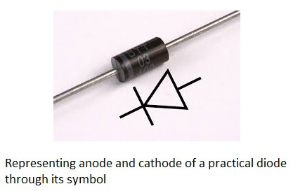
Basic Electronics - Diodes
After having known about various components, let us focus on another important component in the field of electronics, known as a Diode. A semiconductor diode is a two terminal electronic component with a PN junction. This is also called as a Rectifier.

The anode which is the positive terminal of a diode is represented with A and the cathode, which is the negative terminal is represented with K. To know the anode and cathode of a practical diode, a fine line is drawn on the diode which means cathode, while the other end represents anode.
As we had already discussed about the P-type and N-type semiconductors, and the behavior of their carriers, let us now try to join these materials together to see what happens.
Formation of a Diode
If a P-type and an N-type material are brought close to each other, both of them join to form a junction, as shown in the figure below.

A P-type material has holes as the majority carriers and an N-type material has electrons as the majority carriers. As opposite charges attract, few holes in P-type tend to go to n-side, whereas few electrons in N-type tend to go to P-side.
As both of them travel towards the junction, holes and electrons recombine with each other to neutralize and forms ions. Now, in this junction, there exists a region where the positive and negative ions are formed, called as PN junction or junction barrier as shown in the figure.

The formation of negative ions on P-side and positive ions on N-side results in the formation of a narrow charged region on either side of the PN junction. This region is now free from movable charge carriers. The ions present here have been stationary and maintain a region of space between them without any charge carriers.
As this region acts as a barrier between P and N type materials, this is also called as Barrier junction. This has another name called as Depletion region meaning it depletes both the regions. There occurs a potential difference VD due to the formation of ions, across the junction called as Potential Barrier as it prevents further movement of holes and electrons through the junction.
Biasing of a Diode
When a diode or any two-terminal component is connected in a circuit, it has two biased conditions with the given supply. They are Forward biased condition and Reverse biased condition. Let us know them in detail.
Forward Biased Condition
When a diode is connected in a circuit, with its anode to the positive terminal and cathode to the negative terminal of the supply, then such a connection is said to be forward biased condition. This kind of connection makes the circuit more and more forward biased and helps in more conduction. A diode conducts well in forward biased condition.
Reverse Biased Condition
When a diode is connected in a circuit, with its anode to the negative terminal and cathode to the positive terminal of the supply, then such a connection is said to be Reverse biased condition. This kind of connection makes the circuit more and more reverse biased and helps in minimizing and preventing the conduction. A diode cannot conduct in reverse biased condition.

Let us now try to know what happens if a diode is connected in forward biased and in reverse biased conditions.
Working under Forward Biased
When an external voltage is applied to a diode such that it cancels the potential barrier and permits the flow of current is called as forward bias. When anode and cathode are connected to positive and negative terminals respectively, the holes in P-type and electrons in N-type tend to move across the junction, breaking the barrier. There exists a free flow of current with this, almost eliminating the barrier.

With the repulsive force provided by positive terminal to holes and by negative terminal to electrons, the recombination takes place in the junction. The supply voltage should be such high that it forces the movement of electrons and holes through the barrier and to cross it to provide forward current.
Forward Current is the current produced by the diode when operating in forward biased condition and it is indicated by If.
Working under Reverse Biased
When an external voltage is applied to a diode such that it increases the potential barrier and restricts the flow of current is called as Reverse bias. When anode and cathode are connected to negative and positive terminals respectively, the electrons are attracted towards the positive terminal and holes are attracted towards the negative terminal. Hence both will be away from the potential barrier increasing the junction resistance and preventing any electron to cross the junction.
The following figure explains this. The graph of conduction when no field is applied and when some external field is applied are also drawn.

With the increasing reverse bias, the junction has few minority carriers to cross the junction. This current is normally negligible. This reverse current is almost constant when the temperature is constant. But when this reverse voltage increases further, then a point called reverse breakdown occurs, where an avalanche of current flows through the junction. This high reverse current damages the device.
Reverse current is the current produced by the diode when operating in reverse biased condition and it is indicated by Ir. Hence a diode provides high resistance path in reverse biased condition and doesnt conduct, where it provides a low resistance path in forward biased condition and conducts. Thus we can conclude that a diode is a one-way device which conducts in forward bias and acts as an insulator in reverse bias. This behavior makes it work as a rectifier, which converts AC to DC.
Peak Inverse Voltage
Peak Inverse Voltage is shortly called as PIV. It states the maximum voltage applied in reverse bias. The Peak Inverse Voltage can be defined as The maximum reverse voltage that a diode can withstand without being destroyed. Hence, this voltage is considered during reverse biased condition. It denotes how a diode can be safely operated in reverse bias.
Purpose of a Diode
A diode is used to block the electric current flow in one direction, i.e. in forward direction and to block in reverse direction. This principle of diode makes it work as a Rectifier.
For a circuit to allow the current flow in one direction but to stop in the other direction, the rectifier diode is the best choice. Thus the output will be DC removing the AC components. The circuits such as half wave and full wave rectifiers are made using diodes, which can be studied in Electronic Circuits tutorials.
A diode is also used as a Switch. It helps a faster ON and OFF for the output that should occur in a quick rate.
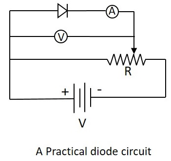
V - I Characteristics of a Diode
A Practical circuit arrangement for a PN junction diode is as shown in the following figure. An ammeter is connected in series and voltmeter in parallel, while the supply is controlled through a variable resistor.
During the operation, when the diode is in forward biased condition, at some particular voltage, the potential barrier gets eliminated. Such a voltage is called as Cut-off Voltage or Knee Voltage. If the forward voltage exceeds beyond the limit, the forward current rises up exponentially and if this is done further, the device is damaged due to overheating.
The following graph shows the state of diode conduction in forward and reverse biased conditions.

During the reverse bias, current produced through minority carriers exist known as Reverse current. As the reverse voltage increases, this reverse current increases and it suddenly breaks down at a point, resulting in the permanent destruction of the junction.