
 Data Structure
 Networking
 RDBMS
RDBMS Operating System
 Java
Java MS Excel
 iOS
iOS HTML
HTML CSS
CSS Android
 Python
 C Programming
 C++
C++ C#
C# MongoDB
 MySQL
MySQL Javascript
 PHP
PHP
- Selected Reading
- UPSC IAS Exams Notes
- Developer's Best Practices
- Questions and Answers
- Effective Resume Writing
- HR Interview Questions
- Computer Glossary
- Who is Who
SIM instruction in 8085
In 8085 Instruction set, SIM stands for “SetInterrupt Mask”. It is 1-Byte instruction and it is a multi-purpose instruction. The main uses of SIM instruction are –
Masking/unmasking of RST7.5, RST6.5, and RST5.5
Reset to 0 RST7.5 flip-flop
Perform serial output of data
| Mnemonics, Operand |
Opcode(in HEX) |
Bytes |
|---|---|---|
| SIM |
30 |
1 |
When SIM instruction is executed then the content of theAccumulator decides the action to be taken. So before executing the SIM instruction, it is mandatory to initialize Accumulator with the required value. The meaning and purpose of the various bits of the accumulator when SIM is executed has been depicted below –
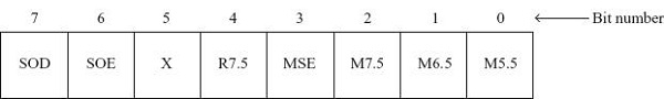
Note that except bit 5, which is a don't care bit, the other bits of the Accumulator decide the effect of executing the SIM instruction. Masking of interrupts: Only the LS 4 bits of the accumulator are used for masking or unmasking of interrupts.
| Bit No. |
Purpose |
|---|---|
| Bit 3: |
This is the Mask Set Enable (MSE) bit. This bit can have two values: 0or 1.
|
| Bit 2: |
This is mask RST7.5 (M7.5) bit. Thisbit is meaningful only if MSE bit = 1. If MSE = 1 and M7.5 = 0,RST7.5 is unmasked. If MSE = 1 and M7.5 = 1, RST7.5 is masked. |
| Bit 1: |
This is M6.5 bit, used for masking/unmasking of RST6.5. It is similar to M7.5 bit. |
| Bit 0: |
This is M5.5 bit, used for masking/unmasking of RST5.5. It is similar to M7.5 bit. |
It should be noted that RST7.5, RST6.5, and RST5.5 can be masked or unmasked using this SIM instruction. TRAP and INTR cannot be masked or unmasked using SIM. TRAP is not allowed to be masked because it is the highest priority un-maskable interrupt. INTR does do not need the facility of masking because it is the lowest priority interrupt. After reset of 8085 RST7.5, RST6.5, and RST5.5 interrupts will be in masked condition.
Reset RST7.5 flip-flop: Bit 4 (R7.5) of Accumulator is used for resetting to 0 RST7.5 flip-flop output when SIM instruction is executed. If R7.5 = 0, SIM instruction is not being used for resetting of RST7.5 flip-flop. Thus, if R7.5 = 0, there is no change in the RST7.5 flip-flop output. If R7.5 = 1, the RST7.5flip-flop gets cleared. Let us consider the following diagram for the better understanding –
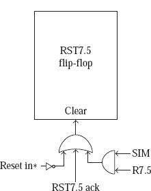
Form the diagram it is clear that SIM signal is activated if and only if, SIM instruction is executed. R7.5 signal is activated when bit 4 (R7.5) of Accumulator = 1. So the RST7.5flip-flop receives logic 1 to its clear input and thus gets cleared when bit 4 of Accumulator = 1 and SIM instruction is executed. Alternatively, RST7.5 flip-flop gets cleared when RST7.5 interrupt is recognized by the 8085 or whenever the 8085 is reset.
In 8085 microprocessor, there is one pin labeled as SOD pin. SOD stands for Serial Output Data. As 8085 is an 8-bit processor, so it generally sends and receives 8-bits of data against each clock pulse. But sometimes parallel communication is not applicable. In those cases, we can select serial communication of8-bit data. That means against each and every clock pulse, 1-bit of information will be transferred. And in this way, it requires 8 clock pulses to transfer 8-bits of data. This is known as serial data communication. Intel 8085 provides SOD (serial output of data) pin and SIM instruction to facilitate serial output of data. The most significant bit of the Accumulator comes out on the SOD pin when the user commands the 8085 to send out the data. The user commands the8085 to send out the MS bit of Accumulator by making bit 6 of Accumulator as 1 and executing the SIM instruction. Consider the following table –
| Bit No. |
Purpose |
|---|---|
| Bit 6: |
This is the serial output enables (SOE) bit. If this bit = 0, SIM instruction is not being used for serial output of data. In such a case, the MS bit of Accumulator is not having any useful information. If SOE bit = 1, the SIM instruction is used for serial output of data. Then the MS bit provides the data to be sent out on the SOD pin of 8085. |
| Bit 7: |
This is serial output data (SOD)bit. This bit is meaningful only if SOE bit = 1. If SOE = 1 and SIM instruction is executed, then the SOD bit comes out on the SOD pin of 8085. |
Let us consider the following program segment –
| Address |
Hex Codes |
Mnemonic |
Comment |
|---|---|---|---|
| 2000 |
3E |
MVI A, 19H |
A ← 19H =0001 1001, it means SOD=0, SDE=0, R7.5=1, MSE=1, M5.5=1 |
| 2001 |
19 |
|
Accumulator value 19H |
| 2002 |
30 |
SIM |
Set Interrupt Mask |
The timing diagram against this instruction SIM execution is as follows –
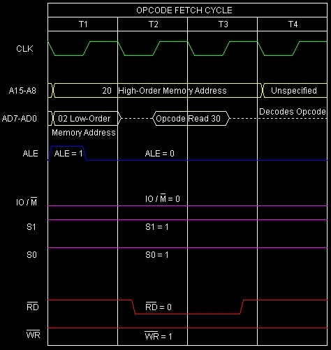
Summary − So this instruction SIM requires 1-Byte, 1-Machine Cycle (Opcode Fetch) and 4 T-States for execution as shown in the timing diagram.

9K+ Views
