
Article Categories
- All Categories
-
 Data Structure
-
 Networking
-
 RDBMS
RDBMS
-
 Operating System
-
 Java
Java
-
 MS Excel
-
 iOS
iOS
-
 HTML
HTML
-
 CSS
CSS
-
 Android
-
 Python
-
 C Programming
-
 C++
C++
-
 C#
C#
-
 MongoDB
-
 MySQL
MySQL
-
 Javascript
-
 PHP
PHP
-
 Economics & Finance
Selected Reading
Description of the pins of 8257
The 8257 pins are described is given in the table below.
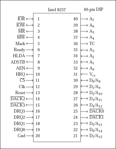
Fig. Physical pin diagram of Intel 8257
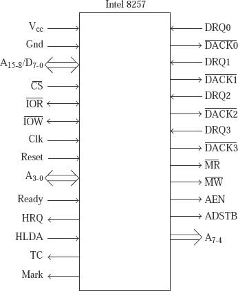
Fig: Functional pin diagram of Intel 8257
8257 is using a power of 5V.
| D7-0/A15-8 |
For communicating with the processor there are 8 bidirectional data pins, when the processor is in active and the 8257 s active state it is in slave mode. When the processor remains in the HOLD state and 8257 behaves as the master, they are used to send out the Most Significant 8 bits of memory address. |
||||||||||||||||||||||
| A3-0 |
When the processor remains in active state and are used as address input pins of 8257. Hence to select one of the registers inside the 8257 the pins are used.
|
||||||||||||||||||||||
| RESET |
RESET is an active high input pin which is connected to the RESET OUTpin of 8085. After 8257 is reset, the control register contents turn to 00H. It means:
|
||||||||||||||||||||||
| DRQ3-0 |
These pins are active high DMA request input pins, assigned to one for each DMA channel. These are activated by some special-purposeI/O port chips like Intel 8257 floppy disk controller, and Intel8275 CRT controller. In fixed priority mode (when RTPR bit is 0 in the control register), DRQ0 has the highest, and DRQ3 the lowest priority. |
||||||||||||||||||||||
| DACK3-0* |
These are the active low DMA acknowledged output pins, only for one for every four DMA channels, Intel 8275. |
||||||||||||||||||||||
| IOR* |
It is an active low input pin which is activated by the processor to read an Address Register, Counter Register, or the status register, when the 8257 works in the slave mode. |
||||||||||||||||||||||
| IOW* |
It is an active low input pin which is activated by the processor to write to an Address Register, Counter Register, or the control register, when the 8257 remains in the slave mode. |
||||||||||||||||||||||
| MR* |
It is an active low output pin which operates tristate when 8257 is in the slave mode. When the processor remains in the HOLD state,8257 drives the pin. |
||||||||||||||||||||||
| MW* |
It is also an active low output pin which is in tristate when 8257 is in the slave mode. When the processor is in the HOLD state, 8257drives the pin which is activated for a DMA write machine cycle and becomes inactive for DMA read machine cycle. |
||||||||||||||||||||||
| CS* |
Unlike others it is also an active low input pin for selecting chip |
||||||||||||||||||||||
| Clk |
It is the input pin of the clock. The maximum allowed frequency for this clock is about 3 MHz. The input of the clock is connected to the output of 8085 in a system which is based on 8085. |
||||||||||||||||||||||
| Ready |
Ready is an active high input pin which has similar function like the ready input of 8085. Devices having slow access times can use it to insert wait states during the DMA read or write to the machine cycles. |
||||||||||||||||||||||
| HRQ |
HRQ is for HOLD request which is an active high output pin also connected to the HOLD input of 8085. Whenever a DRQ input is inactive state, and the DMA channel corresponding to it is enabled, the HRQ output becomes activated by 8257 which essentially requests the processor to grant the total control of the system bus. |
||||||||||||||||||||||
| HLDA |
HLDA means HOLD acknowledge which is an active high input pin, that is connected to the HLDA output of 8085. |
||||||||||||||||||||||
| TC |
TC means terminal count which is an active high output pin. The output becomes activated when all the 14 Least Significant bits of the Control Register become 0 for the DMA channel which is getting to be serviced. |
||||||||||||||||||||||
| MARK |
This is also an active high output pin which is activated when the Least Significant 7 bits of the Control Register become 0 for the DMA channel which is getting serviced. In other words, we can say that whenever the Least Significant byte of the Control Register which becomes 80H or 00H. |
||||||||||||||||||||||
| AEN |
AEN stands for address enable. It is an active high output pin. Intel8257 gives an outputs 0 on AEN when 8085 becomes the master of the computer system. |
||||||||||||||||||||||
| ADSTB |
ADSTB signifies address strobe which is an active high output pin performing the same function to output of 8085. In Intel 8257, if there is output on this pin as 0, if it is in the slave mode.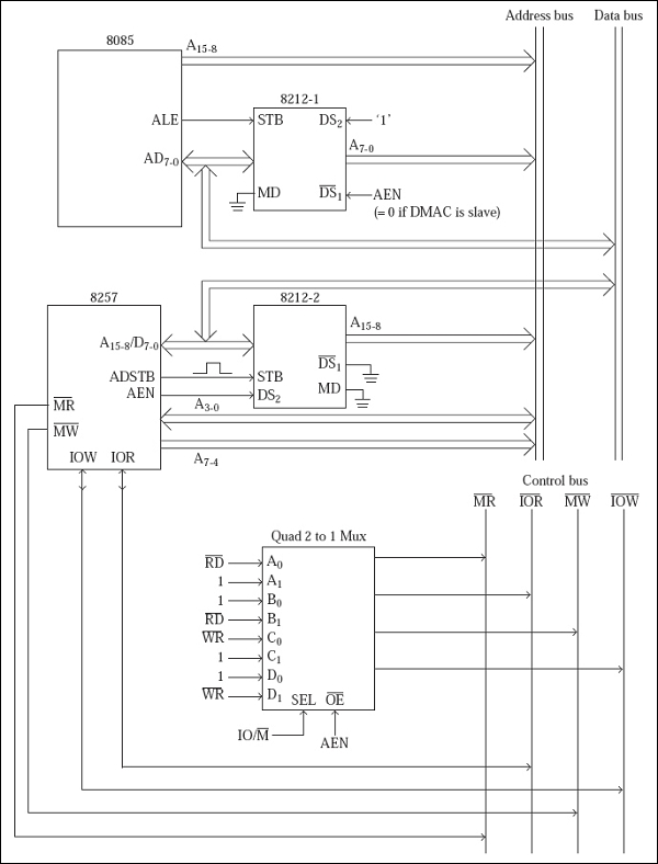 Fig: The block diagram showing the interfacing of 8257 in a based system of 8085 Fig: The block diagram showing the interfacing of 8257 in a based system of 8085
|

Updated on: 2019-07-30T22:30:24+05:30
3K+ Views

Advertisements