- Digital Electronics - Home
- Digital Electronics Basics
- Types of Digital Systems
- Types of Signals
- Logic Levels And Pulse Waveforms
- Digital System Components
- Digital Logic Operations
- Digital Systems Advantages
- Number Systems
- Number Systems
- Binary Numbers Representation
- Binary Arithmetic
- Signed Binary Arithmetic
- Octal Arithmetic
- Hexadecimal Arithmetic
- Complement Arithmetic
- Base Conversions
- Base Conversions
- Binary to Decimal Conversion
- Decimal to Binary Conversion
- Binary to Octal Conversion
- Octal to Binary Conversion
- Octal to Decimal Conversion
- Decimal to Octal Conversion
- Hexadecimal to Binary Conversion
- Binary to Hexadecimal Conversion
- Hexadecimal to Decimal Conversion
- Decimal to Hexadecimal Conversion
- Octal to Hexadecimal Conversion
- Hexadecimal to Octal Conversion
- Binary Codes
- Binary Codes
- 8421 BCD Code
- Excess-3 Code
- Gray Code
- ASCII Codes
- EBCDIC Code
- Code Conversion
- Error Detection & Correction Codes
- Logic Gates
- Logic Gates
- AND Gate
- OR Gate
- NOT Gate
- Universal Gates
- XOR Gate
- XNOR Gate
- CMOS Logic Gate
- OR Gate Using Diode Resistor Logic
- AND Gate vs OR Gate
- Two Level Logic Realization
- Threshold Logic
- Boolean Algebra
- Boolean Algebra
- Laws of Boolean Algebra
- Boolean Functions
- DeMorgan's Theorem
- SOP and POS Form
- POS to Standard POS Form
- Minimization Techniques
- K-Map Minimization
- Three Variable K-Map
- Four Variable K-Map
- Five Variable K-Map
- Six Variable K-Map
- Don't Care Condition
- Quine-McCluskey Method
- Min Terms and Max Terms
- Canonical and Standard Form
- Max Term Representation
- Simplification using Boolean Algebra
- Combinational Logic Circuits
- Digital Combinational Circuits
- Digital Arithmetic Circuits
- Multiplexers
- Multiplexer Design Procedure
- Mux Universal Gate
- 2-Variable Function Using 4:1 Mux
- 3-Variable Function Using 8:1 Mux
- Demultiplexers
- Mux vs Demux
- Parity Bit Generator and Checker
- Comparators
- Encoders
- Keyboard Encoders
- Priority Encoders
- Decoders
- Arithmetic Logic Unit
- 7-Segment LED Display
- Code Converters
- Code Converters
- Binary to Decimal Converter
- Decimal to BCD Converter
- BCD to Decimal Converter
- Binary to Gray Code Converter
- Gray Code to Binary Converter
- BCD to Excess-3 Converter
- Excess-3 to BCD Converter
- Adders
- Half Adders
- Full Adders
- Serial Adders
- Parallel Adders
- Full Adder using Half Adder
- Half Adder vs Full Adder
- Full Adder with NAND Gates
- Half Adder with NAND Gates
- Binary Adder-Subtractor
- Subtractors
- Half Subtractors
- Full Subtractors
- Parallel Subtractors
- Full Subtractor using 2 Half Subtractors
- Half Subtractor using NAND Gates
- Sequential Logic Circuits
- Digital Sequential Circuits
- Clock Signal and Triggering
- Latches
- Shift Registers
- Shift Register Applications
- Binary Registers
- Bidirectional Shift Register
- Counters
- Binary Counters
- Non-binary Counter
- Design of Synchronous Counter
- Synchronous vs Asynchronous Counter
- Finite State Machines
- Algorithmic State Machines
- Flip Flops
- Flip-Flops
- Conversion of Flip-Flops
- D Flip-Flops
- JK Flip-Flops
- T Flip-Flops
- SR Flip-Flops
- Clocked SR Flip-Flop
- Unclocked SR Flip-Flop
- Clocked JK Flip-Flop
- JK to T Flip-Flop
- SR to JK Flip-Flop
- Triggering Methods:Flip-Flop
- Edge-Triggered Flip-Flop
- Master-Slave JK Flip-Flop
- Race-around Condition
- A/D and D/A Converters
- Analog-to-Digital Converter
- Digital-to-Analog Converter
- DAC and ADC ICs
- Realization of Logic Gates
- NOT Gate from NAND Gate
- OR Gate from NAND Gate
- AND Gate from NAND Gate
- NOR Gate from NAND Gate
- XOR Gate from NAND Gate
- XNOR Gate from NAND Gate
- NOT Gate from NOR Gate
- OR Gate from NOR Gate
- AND Gate from NOR Gate
- NAND Gate from NOR Gate
- XOR Gate from NOR Gate
- XNOR Gate from NOR Gate
- NAND/NOR Gate using CMOS
- Full Subtractor using NAND Gate
- AND Gate Using 2:1 MUX
- OR Gate Using 2:1 MUX
- NOT Gate Using 2:1 MUX
- Memory Devices
- Memory Devices
- RAM and ROM
- Cache Memory Design
- Programmable Logic Devices
- Programmable Logic Devices
- Programmable Logic Array
- Programmable Array Logic
- Field Programmable Gate Arrays
- Digital Electronics Families
- Digital Electronics Families
- CPU Architecture
- CPU Architecture
Clocked JK Flip-Flop
In digital electronics, a flip-flop is a most fundamental memory element used in several electronic circuit to store 1-bit information. A flip-flop is a basically a bistable multivibrator having two stable states.
Flip-flops are made up of a combination of logic gates. However, a logic gate itself cannot store information, but when several logic gates are connected in a specific manner, they can store information. Also, flip-flop is the most elementary building block of all sequential logic circuits. The block diagram representation of a flip-flop is shown in Figure-1.
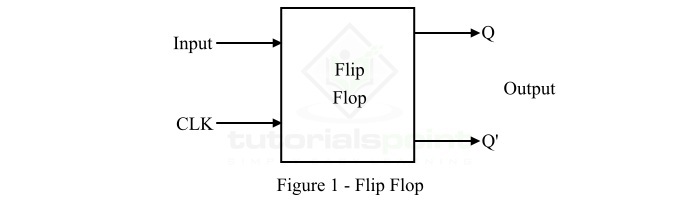
A flip-flop has one or more inputs and two outputs, usually represented by Q and Q' along with a clock input. The clock input is used to trigger the flip-flop so that it can change states of its outputs.
There are several types of flip-flops such as SR flip-flop, JK flip-flop, D flip-flop, and T flip-flop. Each type of flip-flop has its unique properties and characteristics needed for a particular purpose.
This is article is meant for explaining the circuit diagram, truth table, and Boolean expression of the clocked JK flip-flop. So let us start with the basic introduction of the clocked JK flip-flop.
What is a Clocked JK Flip-Flop?
A flip-flop which has two inputs specified by the two letter J and K respectively is called a JK flip-flop. In the case of JK flip-flip, the symbols J and K are alike to the letter S and R in a SR flip-flop.
Technically, the JK flip-flop is basically a refinement of the SR flip-flop in which the invalid or forbidden state of the SR flip-flop is defined.
The block diagram representation of a JK flip-flop is shown in Figure-2 below.

The logic circuit diagram of the JK flip-flop is shown in Figure-3.
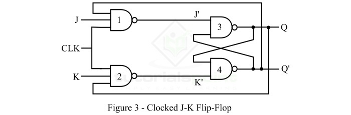
Hence, the JK flip-flop has two inputs labelled as J and K, and two outputs, Q and Q'. It also has an extra input terminal for clock signal. The clock signal is used to synchronize the flip-flop circuit.
The JK flip-flop is named "JK" in the honor of an inventor Jack Kilby who invented the integrated circuit (IC) in 1958.
Operation of Clocked JK Flip-Flop
The operation of the above circuit of clocked JK flip-flop is explained below −
When the clock signal is absent, the circuit will remain inactive and the outputs of NAND gates 3 and 4 do not change with any change in the inputs J and K.
When the clock signal is applied to the circuit, the outputs of the NAND gates 3 and 4 will be as per the inputs J and K. In this case, the circuit will operate as described in the following truth table
| Inputs | Previous State | Output | (Next State) | Comment |
|---|---|---|---|---|
| J | K | Qn | Qn+1 | |
| 0 | 0 | 0 | 0 | No Change |
| 0 | 0 | 1 | 1 | No Change |
| 0 | 1 | 0 | 0 | Reset |
| 0 | 1 | 1 | 0 | Reset |
| 1 | 0 | 0 | 1 | Set |
| 1 | 0 | 1 | 1 | Set |
| 1 | 1 | 0 | 1 | Toggle |
| 1 | 1 | 1 | 0 | Toggle |
From this truth table of the clocked JK flip-flop, we can derive the characteristic equation of the flip-flop as follows −

Hence, the characteristic equation of the JK flip-flop is,
$$\mathrm{Q_{n+1}\:=\:JQ_{n}^{'}\:+\:K'Q_{n}}$$
Advantages of Clocked JK Flip-flop
The following are the major advantages of JK flip-flop
- In JK flip-flop, the forbidden state does not occur.
- In JK flip-flop, instead of forbidden state, the present state toggles, i.e. the present state gets complemented when both the inputs (J and K) are 1.
This is all about the clocked JK flip-flop in digital electronics.